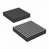
LTM4615IV#PBF Linear Technology, LTM4615IV#PBF Datasheet - Page 15

LTM4615IV#PBF
Manufacturer Part Number
LTM4615IV#PBF
Description
IC SWIT REG BUCK 4A ADJ 144LGA
Manufacturer
Linear Technology
Series
µModuler
Type
Point of Load (POL) Non-Isolatedr
Specifications of LTM4615IV#PBF
Design Resources
LTM4615 Spice Model
Output
0.8 ~ 5 V
Number Of Outputs
3
Power (watts)
12W
Mounting Type
Surface Mount
Voltage - Input
2.38 ~ 5.5 V
Package / Case
144-LGA
1st Output
0.8 ~ 5 VDC @ 4A
2nd Output
0.8 ~ 5 VDC @ 4A
3rd Output
0.8 ~ 5 VDC @ 4A
Size / Dimension
0.59" L x 0.59" W x 0.11" H (15mm x 15mm x 2.8mm)
Power (watts) - Rated
12W
Operating Temperature
-40°C ~ 125°C
Efficiency
95%
Primary Input Voltage
5.5V
No. Of Outputs
3
Output Voltage
5V
Output Current
1.5A
Voltage Regulator Case Style
LGA
No. Of Pins
144
Operating Temperature Range
-40°C To +125°C
Rohs Compliant
Yes
Dc To Dc Converter Type
Step Down
Pin Count
144
Input Voltage
5.5V
Switching Freq
1250KHz
Package Type
LGA
Output Type
Adjustable
Switching Regulator
Yes
Mounting
Surface Mount
Input Voltage (min)
2.375V
Operating Temperature Classification
Automotive
Lead Free Status / RoHS Status
Lead free / RoHS Compliant
Available stocks
Company
Part Number
Manufacturer
Quantity
Price
TYPICAL APPLICATIONS
Thermal Considerations and Output Current Derating
The power loss curves in Figures 5 and 6 can be used
in coordination with the load current derating curves in
Figures 7 to10 for calculating an approximate θ
resistance for the LTM4615 with various heat sinking and
airfl ow conditions. Both of the LTM4615 outputs are at full
4A load current, and the power loss curves in Figures 5
and 6 are combined power losses plotted for both output
voltages up to 4A each. The VLDO regulator is set to have
a power dissipation of a 0.5W since it is generally used
with dropout voltages of 0.5V or less. For example: 1.2V
to 1V, 1.5V to 1V, 1.5V to 1.2V and 1.8V to 1.5V. Other
drop voltages can be supported at VLDO maximum load,
but further thermal analysis will be required for the VLDO.
The 4A output voltages are 1.2V and 3.3V. These voltages
are chosen to include the lower and higher output voltage
ranges for correlating the thermal resistance. Thermal
models are derived from several temperature measure-
ments in a controlled temperature chamber along with
thermal modeling analysis. The junction temperatures are
monitored while ambient temperature is increased with and
without airfl ow. The junctions are maintained at ~120°C
while lowering output current or power while increasing
ambient temperature. The 120°C is chosen to allow for
a 5°C margin window relative to the maximum 125°C.
The decreased output current will decrease the internal
module loss as ambient temperature is increased. The
2.5
2.0
1.5
1.0
0.5
0
0
V
IN
= 5V
Figure 5. 1.2V Power Loss
1
LOAD CURRENT (A)
2
3
4615 F05
4
JA
thermal
power loss curves in Figures 5 and 6 show this amount of
power loss as a function of load current that is specifi ed
for both channels. The monitored junction temperature of
120°C minus the ambient operating temperature specifi es
how much module temperature rise can be allowed. As an
example in Figure 7 the load current is derated to 3A for
each channel with 0LFM at ~90°C and the power loss for
both channels at 5V to 1.2V at 3A output are ~1.4W, then
include the VDLO power loss of 0.5W to equal 1.9W. If the
90°C ambient temperature is subtracted from the 120°C
maximum junction temperature, then the difference of
30°C divided 1.9W equals a 15.7°C/W thermal resistance.
Table 2 specifi es a 15°C/W value which is very close. Table
2 and Table 3 provide equivalent thermal resistances for
1.2V and 3.3V outputs with and without air fl ow and heat
sinking. The combined power loss for the two 4A outputs
plus the VLDO power loss can be summed together and
multiplied by the thermal resistance values in Tables 2
and 3 for module temperature rise under the specifi ed
conditions. The printed circuit board is a 1.6mm thick
four layer board with two ounce copper for the two outer
layers and 1 ounce copper for the two inner layers. The
PCB dimensions are 95mm × 76mm. The BGA heat sinks
are listed below Table 3. The data sheet lists the θ
tion to pin) and θ
under the Pin Confi guration diagram.
3.0
2.5
2.0
1.5
1.0
0.5
0
0
V
IN
JC
= 5V
Figure 6. 3.3V Power Loss
(Junction to case) thermal resistances
1
LOAD CURRENT (A)
2
3
LTM4615
4615 F06
4
JP
15
(Junc-
4615f


