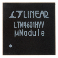
LTM4601HVIV#PBF Linear Technology, LTM4601HVIV#PBF Datasheet - Page 21

LTM4601HVIV#PBF
Manufacturer Part Number
LTM4601HVIV#PBF
Description
IC DC/DC UMODULE 12A 118-LGA
Manufacturer
Linear Technology
Series
µModuler
Type
Point of Load (POL) Non-Isolatedr
Datasheet
1.LTM4601HVEVPBF.pdf
(28 pages)
Specifications of LTM4601HVIV#PBF
Design Resources
LTM4601HV Spice Model
Output
0.6 ~ 5 V
Number Of Outputs
1
Power (watts)
60W
Mounting Type
Surface Mount
Voltage - Input
4.5 ~ 28 V
Package / Case
118-LGA
1st Output
0.6 ~ 5 VDC @ 12A
Size / Dimension
0.59" L x 0.59" W x 0.11" H (15mm x 15mm x 2.8mm)
Power (watts) - Rated
60W
Operating Temperature
-40°C ~ 85°C
Efficiency
95%
Lead Free Status / RoHS Status
Lead free / RoHS Compliant
3rd Output
-
2nd Output
-
Other names
LTM4601HEIV#PBF
LTM4601HEIV#PBF
LTM4601HEIV#PBF
Available stocks
Company
Part Number
Manufacturer
Quantity
Price
APPLICATIONS INFORMATION
Solution
Lower the switching frequency at lower input voltages to
allow for higher duty cycles, and meet the 400ns mini-
mum off-time at 4.5V input voltage. The off-time should
be about 500ns with 100ns guard band. The duty cycle
for (3.3V/4.5) = ~73%. Frequency = (1 – DC)/t
(1 – 0.73)/500ns = 540kHz. The switching frequency
needs to be lowered to 540kHz at 4.5V input. t
frequency, or 1.35μs. The f
is 1/3 of V
the internal 39.2k. The I
10V TO 28V
IN
, and the I
FOR ≥12V INPUT
10μF
V
25V
IN
C2
EFFICIENCY
IMPROVE
fSET
5% MARGIN
fSET
C1
10μF
25V
current equates to 38μA with
100k
392k
current needs to be 24μA for
1%
SET
R2
CMSSH-3C3
R1
V
OUT
DUAL
100k
pin voltage compliance
R4
Figure 18. 5V at 8A Design Without Differential Amplifi er
SOT-323
PGOOD
MPGM
RUN
COMP
INTV
DRV
CC
CC
SGND
V
IN
LTM4601HV
ON
PLLIN
PGND
MARGIN CONTROL
OFF
= DC/
TRACK/SS
, or
f
V
DIFFV
SET
OUT_LCL
MARG0
MARG1
V
V
R
100k
OSNS
OSNS
V
fSET
OUT
OUT
V
FB
+
–
540kHz operation. As shown in Figure 19, a resistor can
be placed from V
current out of the f
=1.5V and V
into the f
This enables the 540kHz operation and the 4.5V to 28V
input operation for down converting to 3.3V output. The
frequency will scale from 540kHz to 1.1 MHz over this
input range. This provides for an effective output current
of 8A over the input range.
TRACK/SS CONTROL
REVIEW TEMPERATURE
DERATING CURVE
8.25k
R
SET
SET
4601HV F18
OUT
node and lower the I
= 3.3V, therefore 130k will source 14μA
OUT
+
SET
C3
100μF
6.3V
SANYO
POSCAP
to f
pin to 24μA. The f
SET
to lower the effective I
22μF
6.3V
LTM4601HV
fSET
V
5V
8A
OUT
current to 24μA.
REFER TO
SET
TABLE 2
pin is 4.5V/3
21
4601hvfa
fSET


