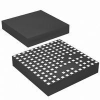
LTM4612MPV#PBF Linear Technology, LTM4612MPV#PBF Datasheet - Page 11

LTM4612MPV#PBF
Manufacturer Part Number
LTM4612MPV#PBF
Description
IC BUCK SYNC ADJ 5A 133LGA
Manufacturer
Linear Technology
Series
µModuler
Type
Point of Load (POL) Non-Isolatedr
Datasheet
1.LTM4612EVPBF.pdf
(26 pages)
Specifications of LTM4612MPV#PBF
Design Resources
LTM4612 Spice Model
Output
3.3 ~ 15 V
Number Of Outputs
1
Power (watts)
75W
Mounting Type
Surface Mount
Voltage - Input
5 ~ 36 V
Package / Case
133-LGA
1st Output
3.3 ~ 15 VDC @ 5A
Size / Dimension
0.59" L x 0.59" W x 0.11" H (15mm x 15mm x 2.8mm)
Power (watts) - Rated
75W
Operating Temperature
-55°C ~ 125°C
Lead Free Status / RoHS Status
Lead free / RoHS Compliant
3rd Output
-
2nd Output
-
Available stocks
Company
Part Number
Manufacturer
Quantity
Price
applicaTions inForMaTion
The typical LTM4612 application circuit is shown in
Figure 18. External component selection is primarily
determined by the maximum load current and output
voltage. Refer to Table 2 for specific external capacitor
requirements for a particular application.
V
There are restrictions in the maximum V
down ratio that can be achieved for a given input voltage.
These constraints are shown in the Typical Performance
Characteristic curve labeled “V
Ratio.” Note that additional thermal derating may be ap-
plied. See the Thermal Considerations and Output Current
Derating section in this data sheet.
Output Voltage Programming and Margining
The PWM controller has an internal 0.6V reference voltage.
As shown in the Block Diagram, a 100k internal feedback
resistor connects the V
resistor, R
the output voltage.
Table 1. R
The MPGM pin programs a current that when multiplied
by an internal 10k resistor sets up the 0.6V reference ±
offset for margining. A 1.18V reference divided by the
R
Calculate V
Where %V
and V
Where R
pin to ground.
R
V
IN
PGM
FB
OUT
R
V
V
to V
OUT
(kW)
OUT MARGIN
PGM
(V)
OUT(MARGIN)
resistor on the MPGM pin programs the current.
OUT
(
=
FB
PGM
=
FB
22.1
0 6
OUT
3.3
Standard 1% Resistor Values vs V
OUT(MARGIN)
V
0 6
.
Stepdown Ratios
, from the V
OUT
.
is the resistor value to place on the MPGM
V
is the percentage of V
V
)
•
13.7
=
•
100
5
is the margin quantity in volts:
V
%
OUT MARGIN
100
R
k R
V
1 18
OUT
OUT
FB
11
+
:
6
.
(
FB
and V
pin to the SGND pin programs
FB
•
V
8.06
V
8
OUT
)
FB
IN
•
6.34
pins together. Adding a
10
10
to V
OUT
k
IN
5.23
OUT
OUT
12
to be margined,
and V
Step-Down
4.42
14
OUT
4.12
step
15
The output margining will be ± margining of the value.
This is controlled by the MARG0 and MARG1 pins. See
the truth table below:
Operating Frequency
The operating frequency of the LTM4612 is optimized to
achieve the compact package size and the minimum
output ripple voltage while still keeping high efficiency.
As shown in Figure 2, the frequency is linearly increased
with larger output voltages to keep the low output cur-
rent ripple. Figure 3 shows the inductor current ripple DI
with different output voltages. In most applications, no
additional frequency adjusting is required.
Figure 3. Inductor Current Ripple vs Output Voltage
MARG1
Figure 2. Operating Frequency vs Output Voltage
HIGH
HIGH
LOW
LOW
1200
1000
800
600
400
200
3.5
3.0
2.5
2.0
1.5
1.0
0.5
2
2
4
4
6
6
MARG0
V
V
8
V
HIGH
HIGH
8
LOW
LOW
OUT
IN
OUT
= 20V
(V)
(V)
10
10
12
12
V
IN
V
= 36V
IN
14
14
= 28V
LTM4612
4612 F02
4612 F03
MARGIN DOWN
16
16
NO MARGIN
MARGIN UP
NO MARGIN
MODE
4612fa


