LSN-T/10-D12-C Murata Power Solutions Inc, LSN-T/10-D12-C Datasheet - Page 4
LSN-T/10-D12-C
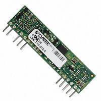
Manufacturer Part Number
LSN-T/10-D12-C
Description
CONV DC/DC 10A 0.75-5.25V SIP
Manufacturer
Murata Power Solutions Inc
Type
Point of Load (POL) Non-Isolatedr
Series
LSNr
Datasheet
1.LSN-T10-D12N-C.pdf
(12 pages)
Specifications of LSN-T/10-D12-C
Number Of Outputs
1
Output
0.75 ~ 5.25V
Power (watts)
51W
Mounting Type
Through Hole
Voltage - Input
10 ~ 14V
Package / Case
11-SIP Module (10 Leads)
1st Output
0.75 ~ 5.25 VDC @ 10A
Size / Dimension
2.00" L x 0.34" W x 0.55" H (50.8mm x 8.6mm x 14mm)
Power (watts) - Rated
51W
Operating Temperature
-40°C ~ 85°C
Efficiency
96.5%
Approvals
EN, UL
Output Power
53 W
Input Voltage Range
10.8 V to 13.2 V
Input Voltage (nominal)
12 V
Output Voltage (channel 1)
1.2 V to 5.25 V
Output Current (channel 1)
10 A
Package / Case Size
SIP
Output Type
Low Voltage
Output Voltage
0.75 V to 5.25 V
Input Voltage
10V To 14V
Power Rating
51W
Output Current
10A
Supply Voltage
12V
Dc / Dc Converter Case Style
SIP
Dc/dc Converter Mounting
Through Hole
Svhc
No SVHC (15-Dec-2010)
Rohs Compliant
Yes
Product
Non-Isolated / POL
Lead Free Status / RoHS Status
Lead free / RoHS Compliant
3rd Output
-
2nd Output
-
Lead Free Status / Rohs Status
Lead free / RoHS Compliant
Other names
811-1807-5
Available stocks
Company
Part Number
Manufacturer
Quantity
Price
Company:

Part Number:
LSN-T/10-D12-C
Manufacturer:
Murata Power Solutions Inc
Quantity:
135


Return Current Paths
The LSN D12 SIP’s are non-isolated DC/DC converters. Their two Common
pins (pins 5 and 6) are connected to each other internally (see Figure 1). To
the extent possible (with the intent of minimizing ground loops), input return
current should be directed through pin 6 (also referred to as –Input or Input
Return), and output return current should be directed through pin 5 (also
referred to as –Output or Output Return). Any on/off control signals applied to
pin 11 (On/Off Control) should be referenced to Common
(specifically pin 6).
I/O Filtering and Noise Reduction
All models in the LSN D12 Series are tested and specified with external 22μF
tantalum input and 10 || 1μF output capacitors. These capacitors are neces-
sary to accommodate our test equipment and may not be required to achieve
desired performance in your application. The LSN D12's are designed with
high-quality, high-performance internal I/O caps, and will operate within spec
in most applications with no additional external components.
In particular, the LSN D12's input capacitors are specified for low ESR and are
fully rated to handle the units' input ripple currents. Similarly, the internal out-
put capacitors are specified for low ESR and full-range frequency response.
In critical applications, input/output ripple/noise may be further reduced using
filtering techniques, the simplest being the installation of external I/O caps.
External input capacitors serve primarily as energy-storage devices. They
minimize high-frequency variations in input voltage (usually caused by IR
drops in conductors leading to the DC/DC) as the switching converter draws
pulses of current. Input capacitors should be selected for bulk capacitance
(at appropriate frequencies), low ESR, and high rms-ripple-current ratings.
The switching nature of modern DC/DC's requires that the dc input voltage
source have low ac impedance at the frequencies of interest. Highly inductive
source impedances can greatly affect system stability. Your specific system
configuration may necessitate additional considerations.
Output ripple/noise (also referred to as periodic and random deviations or
PARD) may be reduced below specified limits with the installation of additional
external output capacitors. Output capacitors function as true filter elements
and should be selected for bulk capacitance, low ESR, and appropriate fre-
quency response. Any scope measurements of PARD should be made directly
at the DC/DC output pins with scope probe ground less than 0.5" in length.
All external capacitors should have appropriate voltage ratings and be located
as close to the converters as possible. Temperature variations for all relevant
parameters should be taken into consideration.
The most effective combination of external I/O capacitors will be a function
of your line voltage and source impedance, as well as your particular load
and layout conditions. Our Applications Engineers can recommend potential
solutions and discuss the possibility of our modifying a given device’s internal
filtering to meet your specific requirements. Contact our Applications Engineer-
ing Group for additional details.
Input Fusing
Most applications and or safety agencies require the installation of fuses at
the inputs of power conversion components. LSN D12 Series DC/DC convert-
ers are not internally fused. Therefore, if input fusing is mandatory, either
a normal-blow or a slow-blow fuse with a value no greater than 15 Amps
TECHNICAL NOTES
www.murata-ps.com
Single Adjustable Output, Non-isolated, 12Vin, 10A, SIP, DC/DC Converters
should be installed within the ungrounded input path to the converter.
As a rule of thumb however, we recommend to use a normal-blow or slow-
blow fuse with a typical value of about twice the maximum input current,
calculated at low line with the converters minimum efficiency.
Safety Considerations
LSN D12 SIP's are non-isolated DC/DC converters. In general, all DC/DC's
must be installed, including considerations for I/O voltages and spacing/sepa-
ration requirements, in compliance with relevant safety-agency speci-
fications (usually UL/IEC/EN60950).
In particular, for a non-isolated converter's output voltage to meet SELV (safety
extra low voltage) requirements, its input must be SELV compliant.
If the output needs to be ELV (extra low voltage), the input must be ELV.
Input Overvoltage and Reverse-Polarity Protection
LSN D12 SIP Series DC/DC's do not incorporate either input overvoltage or
input reverse-polarity protection. Input voltages in excess of the specified
absolute maximum ratings and input polarity reversals of longer than "instan-
taneous" duration can cause permanent damage to these devices.
Start-Up Time
The V
ping input voltage crosses the lower limit of the specified input voltage range
and the fully loaded output voltage enters and remains within its specified
accuracy band. Actual measured times will vary with input source impedance,
external input capacitance, and the slew rate and final value of the input volt-
age as it appears to the converter.
The On/Off to V
On/Off Control with the nominal input voltage already applied to the converter.
The specification defines the interval between the time at which the converter
is turned on and the fully loaded output voltage enters and remains within its
specified accuracy band. See Typical Performance Curves.
Installing the Converter
These converters may be installed into either commercial pin sockets on
0.1" centers (similar to those used with through-hole integrated circuits)
or inserted into plated-through holes on the host printed circuit board. Pin
sockets obviously facilitate repair and replacement whereas PCB mounting
is mechanically and electrically more secure. Soldered-down PCB installation
also conducts more heat away from the converter. Consider increasing the
copper etch area near the output pins.
Do not use excessive force when installing these converters. If you are not in-
serting the converter into pin sockets, make sure the holes on the host printed
circuit board are of adequate size and spaced properly. You may bend the pins
slightly to line them up with the PCB holes. Using two needle nose pliers, se-
curely hold the base of the pin with one plier (where it enters the converter’s
PCB or the lead frame) and apply a very small bend with the other plier part
way down the pin length. The two-plier method avoids excessive force on the
converter’s PCB. If pins are bent too far or too great an insertion force is used
during installation, this may cause hidden damage on the converter, possibly
voiding the warranty.
Remote Sense
LSN D12 SIP Series DC/DC converters offer an output sense function on pin 3.
IN
to V
OUT
Start-Up Time is the interval between the time at which a ram-
OUT
Start-Up Time assumes the converter is turned off via the
Technical enquiries email: sales@murata-ps.com, tel:
LSN-T/10-D12
LSN-T10-D12.B01 Page 4 of 12
+1 508 339 3000
Related parts for LSN-T/10-D12-C
Image
Part Number
Description
Manufacturer
Datasheet
Request
R

Part Number:
Description:
CONV DC/DC 10A 0.75-5.25V SIP
Manufacturer:
Murata Power Solutions Inc
Datasheet:

Part Number:
Description:
DC/DC TH 10A-Variable Non-iso
Manufacturer:
Murata Power Solutions Inc
Part Number:
Description:
DC/DC TH 10A-Variable Non-iso
Manufacturer:
Murata Power Solutions Inc

Part Number:
Description:
DC/DC TH 10A-Variable Non-iso
Manufacturer:
Murata Power Solutions Inc
Part Number:
Description:
DC/DC TH 10A-Variable Non-iso
Manufacturer:
Murata Power Solutions Inc

Part Number:
Description:
DC/DC TH 16A 12 To 0.75-5.0V Non-Iso
Manufacturer:
Murata Power Solutions Inc
Datasheet:
Part Number:
Description:
DC/DC TH 16A 12 To 0.75-5.0V Non-Iso
Manufacturer:
Murata Power Solutions Inc
Datasheet:
Part Number:
Description:
DC/DC TH 16A 12 To 0.75-5.0V Non-Iso
Manufacturer:
Murata Power Solutions Inc
Datasheet:

Part Number:
Description:
DC/DC TH 16A W3 To 0.75-3.3V Non-Iso
Manufacturer:
Murata Power Solutions Inc
Datasheet:
Part Number:
Description:
DC/DC TH 16A W3 To 0.75-3.3V H Non-Iso
Manufacturer:
Murata Power Solutions Inc
Datasheet:

Part Number:
Description:
Transformers 5Vin 5Vout 200mA 4000Vdc 1:1.33 turn
Manufacturer:
Murata Power Solutions Inc
Datasheet:
Part Number:
Description:
POWER SUPPLY
Manufacturer:
Murata Power Solutions Inc
Datasheet:

Part Number:
Description:
DPM LED MINI 2VDC 3.5DIG LP RED
Manufacturer:
Murata Power Solutions Inc
Datasheet:

Part Number:
Description:
CONV DC/DC 1W 5VIN 5VOUT SIP SGL
Manufacturer:
Murata Power Solutions Inc
Datasheet:

Part Number:
Description:
CONV DC/DC 1W 5VIN 3.3V SIP SGL
Manufacturer:
Murata Power Solutions Inc
Datasheet: