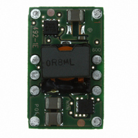
MPDTH03060YAS Murata Electronics North America, MPDTH03060YAS Datasheet - Page 2
MPDTH03060YAS
Manufacturer Part Number
MPDTH03060YAS
Description
CONV DC/DC 18W .55-1.8VOUT 10A
Manufacturer
Murata Electronics North America
Series
MPDr
Type
Point of Load (POL) Non-Isolatedr
Datasheet
1.MPDTH03060YAS.pdf
(10 pages)
Specifications of MPDTH03060YAS
Output
0.55 ~ 1.8V
Number Of Outputs
1
Power (watts)
18W
Mounting Type
Surface Mount
Voltage - Input
2.95 ~ 3.65V
Package / Case
10-DIP SMD Module
1st Output
0.55 ~ 1.8 VDC @ 10A
Size / Dimension
0.99" L x 0.62" W x 0.38" H (25.3mm x 15.8mm x 9.6mm)
Power (watts) - Rated
18W
Operating Temperature
-40°C ~ 85°C
Efficiency
86%
Lead Free Status / RoHS Status
Lead free / RoHS Compliant
3rd Output
-
2nd Output
-
Other names
490-5074
MPDTH03060YAS
MPDTH03060YAS


1. This datasheet is downloaded from the website of Murata Manufacturing co., ltd. Therefore, it’ s specifications are subject to change or our
2. This datasheet has only typical specifications because there is no space for detailed specifications. Therefore, please approve our product
10-A, 3.3-V Input Non-Isolated DDR/QDR
Memory Bus Termination Module
Note:
Ordering Information
Output Voltage (MPDTH03060□xx)
Code
Pin Description
Vin: The positive input voltage power node to the module,
which is referenced to common GND.
VTT: This is the regulated power output from the module with
respect to the GND node, and the tracking
termination supply for the application data and address buses. It
is precisely regulated to the voltage applied to the module's Vref
input, and is active about 20 ms after a valid input source is
applied to the module.
Once active it will track the voltage applied at Vref.
GND: This is the common ground connection for the
VIN and VTT power connections. It is also the 0 VDC
reference for the control inputs.
Inhibit: The Inhibit pin is an open-collector/drain negative logic
input that is referenced to GND. Applying a low-level
ground signal to this input turns off the output voltage, VTT.
Although the module is inhibited, a voltage, VDDQ
will be present at the output terminals, fed through the DDR
memory. When the Inhibit is active, the input current drawn by
the regulator is significantly reduced. If the Inhibit pin is left open
circuit, the module will
produce an output whenever a valid input source is applied. See
the Typical DDR Application Diagram in the
Application Information section for reference.
products in it may be discontinued without advance notice. Please check with our sales representatives or product engineers before ordering.
specifications or transact the approval sheet for product specifications before ordering.
Y
Notes
0.55V-1.8V(Adjustable)
Voltage
(1) Pb free (Sn-Ag-Cu) pin solder material.
Vref: The module senses the voltage at this input to regulate
the output voltage, VTT. The voltage at Vref is also
the
comparators. It is normally set to precisely half the bus
Vref 8 driver supply voltage (VDDQ÷ 2), using a resistor
divider. The Thevenin impedance of the network driving the
Vref pin should not exceed 500 Ω. See the Typical DDR
Application Diagram in the Application Information
section for reference.
Vo Sense: The sense input allows the regulation circuit to
compensate for voltage drop between the module and
the load. For optimal voltage accuracy Vo Sense should
be connected to VTT.
No Connect: No connection.
Package Options (MPDTH03060x□□)
AH
Code
AS
reference
voltage
Description
Horiz. T/H
SMD(*1)
for
the
system
MPDTH03060Y** Application
bus
receiver
2006.10.2
2
Related parts for MPDTH03060YAS
Image
Part Number
Description
Manufacturer
Datasheet
Request
R

Part Number:
Description:
BUZZER PIEZO 25VP-P SMD
Manufacturer:
Murata Electronics North America

Part Number:
Description:
CAP 4-ARRAY 680PF 100V X7R 1206
Manufacturer:
Murata Electronics North America
Datasheet:
Part Number:
Description:
CAP 4-ARRAY 1000PF 100V X7R 1206
Manufacturer:
Murata Electronics North America
Datasheet:
Part Number:
Description:
CAP 4-ARRAY 1800PF 100V X7R 1206
Manufacturer:
Murata Electronics North America
Datasheet:
Part Number:
Description:
CAP 4-ARRAY 68000PF 16V X7R 1206
Manufacturer:
Murata Electronics North America
Datasheet:

Part Number:
Description:
CAP CER 1000PF 50V 10% X7R 0402
Manufacturer:
Murata Electronics North America
Datasheet:
Part Number:
Description:
CAP CER 10000PF 16V 10% X7R 0402
Manufacturer:
Murata Electronics North America
Datasheet:

Part Number:
Description:
CAP 5.5-25PF 2.5X3.2MM SMD
Manufacturer:
Murata Electronics North America
Datasheet:

Part Number:
Description:
CAP 4.5-20PF 2.5X3.2MM SMD
Manufacturer:
Murata Electronics North America
Datasheet:

Part Number:
Description:
CAP 5.0-20PF 3.2X4.5MM SMD RED
Manufacturer:
Murata Electronics North America
Datasheet:

Part Number:
Description:
CAP 2.0-6.0PF 3.2X4.5MM SMD BLU
Manufacturer:
Murata Electronics North America
Datasheet:

Part Number:
Description:
CAP 1.4-3.0PF 3.2X4.5MM SMD BRN
Manufacturer:
Murata Electronics North America
Datasheet:

Part Number:
Description:
CAP 3.0-10PF 3.2X4.5MM SMD WHT
Manufacturer:
Murata Electronics North America
Datasheet:

Part Number:
Description:
CAP 2.0-6.0PF 4X4.5MM TOPADJ BLU
Manufacturer:
Murata Electronics North America
Datasheet:

Part Number:
Description:
CAP 8.5-40PF 4X4.5MM TOPADJ YEL
Manufacturer:
Murata Electronics North America
Datasheet: