LTM4600IV#2DHPBF Linear Technology, LTM4600IV#2DHPBF Datasheet - Page 16
LTM4600IV#2DHPBF
Manufacturer Part Number
LTM4600IV#2DHPBF
Description
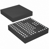
IC DC/DC UMODULE 10A 104-LGA
Manufacturer
Linear Technology
Series
µModuler
Type
Point of Load (POL) Non-Isolatedr
Datasheet
1.LTM4600EVPBF.pdf
(24 pages)
Specifications of LTM4600IV#2DHPBF
Output
0.6 ~ 5 V
Number Of Outputs
1
Power (watts)
50W
Mounting Type
Surface Mount
Voltage - Input
4.5 ~ 20V
Package / Case
104-LGA
1st Output
0.6 ~ 5 VDC @ 10A
Size / Dimension
0.59" L x 0.59" W x 0.11" H (15mm x 15mm x 2.8mm)
Power (watts) - Rated
50W
Operating Temperature
-40°C ~ 85°C
Efficiency
92%
Lead Free Status / RoHS Status
Lead free / RoHS Compliant
3rd Output
-
2nd Output
-
Available stocks
Company
Part Number
Manufacturer
Quantity
Price


APPLICATIONS INFORMATION
LTM4600
Layout Checklist/Example
The high integration of the LTM4600 makes the PCB board
layout very simple and easy. However, to optimize its electri-
cal and thermal performance, some layout considerations
are still necessary.
• Use large PCB copper areas for high current path, in-
• Place high frequency ceramic input and output capaci-
• Place a dedicated power ground layer underneath
• To minimize the via conduction loss and reduce module
• Do not put a via directly on pad unless it is capped
• Use a separated SGND ground copper area for com-
Figure 16 gives a good example of the recommended
layout.
16
cluding V
PCB conduction loss and thermal stress
tors next to the V
high frequency noise
the unit
thermal stress, use multiple vias for interconnection
between top layer and other power layers
ponents connected to signal pins. Connect the SGND
to PGND underneath the unit
IN
, PGND and V
IN
, PGND and V
OUT
. It helps to minimize the
OUT
C
IN
pins to minimize
V
PGND
IN
Figure 16. Recommended PCB Layout
LOAD
V
OUT
TOP LAYER
LTM4600 Frequency Adjustment
The LTM4600 is designed to typically operate at 850kHz
across most input and output conditions. The control ar-
chitecture is constant on time valley mode current control.
The f
optional 1000pF capacitor. The switching frequency has
been optimized to maintain constant output ripple over the
operating conditions. The equations for setting the operat-
ing frequency are set around a programmable constant on
time. This on time is developed by a programmable current
into an on board 10pF capacitor that establishes a ramp
that is compared to a voltage threshold equal to the output
voltage up to a 2.4V clamp. This I
I
from V
• 10pF and t
= DC/t
regulator duty cycle is inversely proportional to V
fore the step-down regulator will remain relatively constant
frequency as the duty cycle adjustment takes place with
lowering V
2.4V clamp. This will hold frequency relatively constant
with different output voltages up to 2.4V. The regulator
switching period is comprised of the on time and off time
as depicted in Figure 17.
ON
= (V
ADJ
ON
IN
IN
. The I
to f
pin is typically left open or decoupled with an
– 0.7V)/110k, with the 110k onboard resistor
IN
4600 F16
OFF
ADJ
. The on time is proportional to V
= t
ON
. The on time is equal to t
s
current is proportional to V
– t
ON
. The frequency is equal to: Freq.
ON
current is equal to:
ON
= (V
OUT
IN
, and the
IN
OUT
, there-
up to a
/I
4600fc
ON
)
Related parts for LTM4600IV#2DHPBF
Image
Part Number
Description
Manufacturer
Datasheet
Request
R

Part Number:
Description:
Manufacturer:
Linear Technology Corporation
Datasheet:

Part Number:
Description:
IC DC/DC UMODULE 10A 104-LGA
Manufacturer:
Linear Technology
Datasheet:

Part Number:
Description:
10A High Effi ciency DC/DC ?Module
Manufacturer:
LINER [Linear Technology]
Datasheet:

Part Number:
Description:
IC DC/DC UMODULE 10A 104-LGA
Manufacturer:
Linear Technology
Datasheet:

Part Number:
Description:
CD ROM LINEARVIEW DATASHEETS
Manufacturer:
Linear Technology
Part Number:
Description:
Standalone Linear Li-Ion Battery Charger with Thermal Regulation in ThinSOT
Manufacturer:
Linear Technology Corporation
Datasheet:
Part Number:
Description:
Low noise, high frequency, 8th order linear phase lowpass filter
Manufacturer:
Linear Technology Corporation
Datasheet:
Part Number:
Description:
Manufacturer:
Linear Technology Corporation
Datasheet:
Part Number:
Description:
Manufacturer:
Linear Technology Corporation
Datasheet:
Part Number:
Description:
Manufacturer:
Linear Technology Corporation
Datasheet:
Part Number:
Description:
Manufacturer:
Linear Technology Corporation
Datasheet:
Part Number:
Description:
Manufacturer:
Linear Technology Corporation
Datasheet:
Part Number:
Description:
Manufacturer:
Linear Technology Corporation
Datasheet:
Part Number:
Description:
Manufacturer:
Linear Technology Corporation
Datasheet:
Part Number:
Description:
Dual and Quad, JFET Input Precision High Speed Op Amps
Manufacturer:
Linear Technology Corporation
Datasheet: