AC1059 Analog Devices Inc, AC1059 Datasheet - Page 3
AC1059
Manufacturer Part Number
AC1059
Description
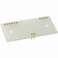
SOCKET FOR MODEL AD210 IC
Manufacturer
Analog Devices Inc
Specifications of AC1059
Accessory Type
Mating Socket
Connector Type
DIP Socket
No. Of Contacts
12
Pitch Spacing
2.54mm
Row Pitch
20.32mm
Contact Termination
Through Hole
Socket Mounting
PC Board
Number Of Contacts
12
Primary Type
AD210
Lead Free Status / RoHS Status
Lead free / RoHS Compliant
For Use With/related Products
AD210
Lead Free Status / RoHS Status
Contains lead / RoHS non-compliant, Lead free / RoHS Compliant


INSIDE THE AD210
The AD210 basic block diagram is illustrated in Figure 1.
A +15 V supply is connected to the power port, and
output ports via a 50 kHz carrier frequency. The uncom-
mitted input amplifier can be used to supply gain or buff-
ering of input signals to the AD210. The fullwave
modulator translates the signal to the carrier frequency for
application to transformer T1. The synchronous demodu-
lator in the output port reconstructs the input signal. A
20 kHz, three-pole filter is employed to minimize output
noise and ripple. Finally, an output buffer provides a low
impedance output capable of driving a 2 k load.
USING THE AD210
The AD210 is very simple to apply in a wide range of ap-
plications. Powered by a single +15 V power supply, the
AD210 will provide outstanding performance when used
as an input or output isolator, in single and multichannel
configurations.
Input Configurations: The basic unity gain configura-
tion for signals up to 10 V is shown in Figure 2. Addi-
tional input amplifier variations are shown in the following
figures. For smaller signal levels Figure 3 shows how to
obtain gain while maintaining a very high input impedance.
The high input impedance of the circuits in Figures 2 and
3 can be maintained in an inverting application. Since the
AD210 is a three-port isolator, either the input leads or
the output leads may be interchanged to create the signal
inversion.
REV. A
+V
–V
I
15 V isolated power is supplied to both the input and
COM
V
+IN
–IN
10V
FB
ISS
ISS
SIG
16
17
19
18
14
15
Figure 2. Basic Unity Gain Configuration
SUPPLY
POWER
INPUT
Figure 1. AD210 Block Diagram
17
16
19
18
14
15
+V
–V
ISS
ISS
INPUT
MOD
T2
PWR
OSCILLATOR
30
+15V
30
POWER
POWER
PWR COM
T1
29
OUTPUT
29
DEMOD
FILTER
AD210
+V
–V
OSS
OSS
T3
AD210
OUTPUT
SUPPLY
POWER
1
4
2
3
( 10V)
1
3
4
2
V
V
OUT
OUT
+V
V
O
–V
O
COM
OSS
OSS
–3–
Figure 4 shows how to accommodate current inputs or sum cur-
rents or voltages. This circuit configuration can also be used for
signals greater than 10 V. For example, a 100 V input span
can be handled with R
Adjustments
When gain and offset adjustments are required, the actual cir-
cuit adjustment components will depend on the choice of input
configuration and whether the adjustments are to be made at
the isolator’s input or output. Adjustments on the output side
might be used when potentiometers on the input side would
represent a hazard due to the presence of high common-mode
voltage during adjustment. Offset adjustments are best done at
the input side, as it is better to null the offset ahead of the gain.
Figure 5 shows the input adjustment circuit for use when the in-
put amplifier is configured in the noninverting mode. This offset
adjustment circuit injects a small voltage in series with the
V
V
SIG
SIG
Figure 4. Summing or Current Input Configuration
LO
HI
I
S
V
R
V
Figure 5. Adjustments for Noninverting Input
OUT
S2
S2
200
= –R
R
R
47.5k
Figure 3. Input Configuration for G > 1
50k
R
G
G
F
R
V
F
S1
S1
OFFSET
(
16
17
19
18
14
15
R
V
R
5k
F
S1
S1
GAIN
100k
+
16
17
19
18
14
15
+V
–V
V
R
S2
F
S2
17
16
19
18
14
15
ISS
ISS
= 20 k and R
+ I
+V
–V
S
ISS
ISS
+ ...
+V
–V
ISS
ISS
+15V
)
30
+15V
30
29
+15V
30
S1
29
= 200 k .
AD210
+V
–V
29
OSS
OSS
AD210
+V
–V
OSS
OSS
AD210
+V
–V
AD210
1
4
2
3
OSS
OSS
V
= V
OUT
1
4
2
3
SIG
V
1
4
2
3
(
1+
OUT
R
R
V
G
F
OUT
)
Related parts for AC1059
Image
Part Number
Description
Manufacturer
Datasheet
Request
R

Part Number:
Description:
±1.7g Dual-Axis IMEMS Accelerometer Evaluation Board
Manufacturer:
Analog Devices Inc
Datasheet:

Part Number:
Description:
Inertial Sensor Evaluation System
Manufacturer:
Analog Devices Inc
Datasheet:
Part Number:
Description:
Manufacturer:
Analog Devices Inc
Datasheet:
Part Number:
Description:
Manufacturer:
Analog Devices Inc
Datasheet:
Part Number:
Description:
Manufacturer:
Analog Devices Inc
Datasheet:
Part Number:
Description:
Manufacturer:
Analog Devices Inc
Datasheet:
Part Number:
Description:
Manufacturer:
Analog Devices Inc
Datasheet:
Part Number:
Description:
Manufacturer:
Analog Devices Inc
Datasheet:
Part Number:
Description:
Manufacturer:
Analog Devices Inc
Datasheet:
Part Number:
Description:
Manufacturer:
Analog Devices Inc
Datasheet:
Part Number:
Description:
Manufacturer:
Analog Devices Inc
Datasheet:
Part Number:
Description:
Manufacturer:
Analog Devices Inc
Datasheet:
Part Number:
Description:
Manufacturer:
Analog Devices Inc
Datasheet: