C8051T600SDB Silicon Laboratories Inc, C8051T600SDB Datasheet - Page 60
C8051T600SDB
Manufacturer Part Number
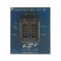
C8051T600SDB
Description
BOARD SOCKET DAUGHTER SOIC
Manufacturer
Silicon Laboratories Inc
Datasheet
1.C8051T600EDB.pdf
(188 pages)
Specifications of C8051T600SDB
Module/board Type
Socket Module - SOIC
Data Bus Width
8 bit
Operating Supply Voltage
+ 1.8 V to + 3.6 V
Lead Free Status / RoHS Status
Contains lead / RoHS non-compliant
For Use With/related Products
C8051T600DK
Lead Free Status / Rohs Status
Lead free / RoHS Compliant
Other names
336-1405


C8051T600/1/2/3/4/5/6
externally driven from –0.25 V to (V
trical specifications are given in Section “8. Electrical Characteristics” on page 30.
The Comparator response time may be configured in software via the CPT0MD register (see SFR Defini-
tion 13.2). Selecting a longer response time reduces the Comparator supply current.
The Comparator hysteresis is software-programmable via its Comparator Control register CPT0CN. The
user can program both the amount of hysteresis voltage (referred to as the input voltage) and the positive
and negative-going symmetry of this hysteresis around the threshold voltage.
The Comparator hysteresis is programmed using Bits3–0 in the Comparator Control Register CPT0CN
(shown in SFR Definition 13.1). The amount of negative hysteresis voltage is determined by the settings of
the CP0HYN bits. As shown in Figure 13.2, settings of 20, 10 or 5 mV of negative hysteresis can be pro-
grammed, or negative hysteresis can be disabled. In a similar way, the amount of positive hysteresis is
determined by the setting the CP0HYP bits.
Comparator interrupts can be generated on both rising-edge and falling-edge output transitions. (For Inter-
rupt enable and priority control, see Section “17.1. MCU Interrupt Sources and Vectors” on page 81). The
CP0FIF flag is set to logic 1 upon a Comparator falling-edge occurrence, and the CP0RIF flag is set to
logic 1 upon the Comparator rising-edge occurrence. Once set, these bits remain set until cleared by soft-
ware.
The output state of the Comparator can be obtained at any time by reading the CP0OUT bit. The Compar-
ator is enabled by setting the CP0EN bit to logic 1, and is disabled by clearing this bit to logic 0.
60
(Programmed with CP0HYP Bits)
Positive Hysteresis Voltage
INPUTS
OUTPUT
VIN+
VIN-
CIRCUIT CONFIGURATION
Positive Hysteresis
CP0-
CP0+
VIN+
VIN-
Disabled
V
OL
Figure 13.2. Comparator Hysteresis Plot
V
OH
+
_
CP0
DD
) + 0.25 V without damage or upset. The complete Comparator elec-
Positive Hysteresis
Maximum
OUT
Rev. 1.2
Negative Hysteresis
Disabled
Negative Hysteresis
(Programmed by CP0HYN Bits)
Maximum
Negative Hysteresis Voltage
Related parts for C8051T600SDB
Image
Part Number
Description
Manufacturer
Datasheet
Request
R

Part Number:
Description:
SMD/C°/SINGLE-ENDED OUTPUT SILICON OSCILLATOR
Manufacturer:
Silicon Laboratories Inc
Part Number:
Description:
Manufacturer:
Silicon Laboratories Inc
Datasheet:
Part Number:
Description:
N/A N/A/SI4010 AES KEYFOB DEMO WITH LCD RX
Manufacturer:
Silicon Laboratories Inc
Datasheet:
Part Number:
Description:
N/A N/A/SI4010 SIMPLIFIED KEY FOB DEMO WITH LED RX
Manufacturer:
Silicon Laboratories Inc
Datasheet:
Part Number:
Description:
N/A/-40 TO 85 OC/EZLINK MODULE; F930/4432 HIGH BAND (REV E/B1)
Manufacturer:
Silicon Laboratories Inc
Part Number:
Description:
EZLink Module; F930/4432 Low Band (rev e/B1)
Manufacturer:
Silicon Laboratories Inc
Part Number:
Description:
I°/4460 10 DBM RADIO TEST CARD 434 MHZ
Manufacturer:
Silicon Laboratories Inc
Part Number:
Description:
I°/4461 14 DBM RADIO TEST CARD 868 MHZ
Manufacturer:
Silicon Laboratories Inc
Part Number:
Description:
I°/4463 20 DBM RFSWITCH RADIO TEST CARD 460 MHZ
Manufacturer:
Silicon Laboratories Inc
Part Number:
Description:
I°/4463 20 DBM RADIO TEST CARD 868 MHZ
Manufacturer:
Silicon Laboratories Inc
Part Number:
Description:
I°/4463 27 DBM RADIO TEST CARD 868 MHZ
Manufacturer:
Silicon Laboratories Inc
Part Number:
Description:
I°/4463 SKYWORKS 30 DBM RADIO TEST CARD 915 MHZ
Manufacturer:
Silicon Laboratories Inc
Part Number:
Description:
N/A N/A/-40 TO 85 OC/4463 RFMD 30 DBM RADIO TEST CARD 915 MHZ
Manufacturer:
Silicon Laboratories Inc
Part Number:
Description:
I°/4463 20 DBM RADIO TEST CARD 169 MHZ
Manufacturer:
Silicon Laboratories Inc