ATAVRDB101 Atmel, ATAVRDB101 Datasheet - Page 6

ATAVRDB101
Manufacturer Part Number
ATAVRDB101
Description
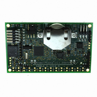
MODULE DISPLAY LCD/RGB BACKLIGHT
Manufacturer
Atmel
Series
AVR®r
Datasheet
1.ATAVRDB101.pdf
(10 pages)
Specifications of ATAVRDB101
Main Purpose
Displays, LCD Controller
Embedded
Yes, MCU, 8-Bit
Utilized Ic / Part
ATmega1281
Primary Attributes
128x64 Pixel, RGB Backlight, Joystick
Secondary Attributes
UART (RS-232), SPI and TWI, Dataflash, Piezo Speaker
Processor To Be Evaluated
ATmega1281
Data Bus Width
8 bit
Interface Type
SPI, TWI, UART
Lead Free Status / RoHS Status
Lead free / RoHS Compliant
Available stocks
Company
Part Number
Manufacturer
Quantity
Price
Company:
Part Number:
ATAVRDB101
Manufacturer:
Atmel
Quantity:
135
2.8 Programming and debugging interface
2.9 Real time clock
2.10 GPIO pins
6
AVR481
The dataflash is connected to the mega1281’s USART0, which can operate in SPI
master mode. The USART0 SPI master communication uses port E, pins 0 to 2. Port
G, pin 5, is used as Chip Select (Slave Select) for the dataflash.
The dataflash is programmed through the mega1281. Please refer to the application
note AVR482 for more information.
The mega1281 can be programmed using either the JTAG or ISP interface.
JTAG programming and debugging can be performed by connecting a JTAGICE mkII
to the 90 degrees pin header J101.
ISP programming can be performed by connecting an ISP enabled AVR programming
tool to the 90 degrees pin header J100. AVR tools like STK500, AVRISP mkII, AVR
Dragon and JTAGICE mkII can be used for this.
Figure 2-6. Pin headers for JTAG (J100) and SPI programming (J101).
A 32kHz crystal is connected to the asynchronous timer of the mega1281. This allows
an application to implement a real time clock (RTC) to keep track of time though sleep
modes are used to reduce the power consumption.
The mega1281 is a high pin count device, and a number of pins are not used. These
are available along the lower edge of the PCB. Be aware that these do NOT have
level converters and should thus not be connected directly to an application board
running on a different voltage level than the DB101.
Table 2-1. Mapping of available IO pins on PCB connectors.
ATmega1281 port pin
PORTB5
PORTB6
PORTD5
PORTD6
PORTD7
PORTC2
PCB connection
J103
J104
J108
J107
J105
J106
8073B-AVR-09/07


