ADCLK905/PCBZ Analog Devices Inc, ADCLK905/PCBZ Datasheet
ADCLK905/PCBZ
Specifications of ADCLK905/PCBZ


Related parts for ADCLK905/PCBZ


ADCLK905/PCBZ Summary of contents
Page 1
FEATURES 95 ps propagation delay 7.5 GHz toggle rate 60 ps typical output rise/fall 60 fs random jitter (RJ) On-chip terminations at both input pins Extended industrial temperature range: −40°C to +125°C 2 3.3 V power supply (V ...
Page 2
ADCLK905/ADCLK907/ADCLK925 TABLE OF CONTENTS Features .............................................................................................. 1 Applications....................................................................................... 1 General Description ......................................................................... 1 Typical Application Circuits........................................................... 1 Revision History ............................................................................... 2 Specifications..................................................................................... 3 Electrical Characteristics............................................................. 3 Absolute Maximum Ratings............................................................ 5 Thermal Resistance ...................................................................... 5 ESD Caution.................................................................................. 5 Pin Configurations and ...
Page 3
SPECIFICATIONS ELECTRICAL CHARACTERISTICS Typical (Typ) values are given for V − given over the full V − 3.3 V ± 10% and Table 1. Parameter DC INPUT CHARACTERISTICS Input Voltage High Level Input ...
Page 4
ADCLK905/ADCLK907/ADCLK925 Parameter POWER SUPPLY Supply Voltage Requirement Power Supply Current ADCLK905 Negative Supply Current Positive Supply Current ADCLK907 Negative Supply Current Positive Supply Current ADCLK925 Negative Supply Current Positive Supply Current 1 Power Supply Rejection 2 Output Swing Supply Rejection ...
Page 5
ABSOLUTE MAXIMUM RATINGS Table 2. Parameter Supply Voltage V − Input Voltage D (D1, D2), D (D1, D2) D1, D2, D1 Pin T (CML or PECL Termination) D (D1, D2 (D1, D2) ...
Page 6
ADCLK905/ADCLK907/ADCLK925 PIN CONFIGURATIONS AND FUNCTION DESCRIPTIONS Table 4. Pin Function Descriptions for 1:1 ADCLK905 Buffer Pin No. Mnemonic Description 1 D Noninverting Input Inverting Input Connect. No physical connection to the die. ...
Page 7
Pin No. Mnemonic Description 10 Q2 Noninverting Output Inverting Output Noninverting Output Reference Voltage 1. Reference voltage for biasing ac-coupled inputs, Channel 1. REF Center Tap 1. ...
Page 8
ADCLK905/ADCLK907/ADCLK925 TYPICAL PERFORMANCE CHARACTERISTICS 25°C, outputs terminated 50 Ω 2.37V Q Q 1.37V 200ps/DIV Figure 7. Output Waveform, V –90 AGILENT E5500 CARRIER: 122.88MHz NO ...
Page 9
SUPPLY VOLTAGE (V) Figure 13. V vs. Power Supply Voltage OD 0.07 0.06 +125°C 0.05 +25°C –55°C 0.04 0.03 +125°C 0.02 +25°C –55°C 0.01 0 2.5 ...
Page 10
ADCLK905/ADCLK907/ADCLK925 Figure 19. 2.488 Gbps PRBS 2 − 1 with OC-48/STM-16 Mask, Measured p-p Jitter 8.1 ps, Source p-p Jitter 3 Figure 20. 9.95 Gbps PRBS 2 − 1 ...
Page 11
APPLICATIONS INFORMATION POWER/GROUND LAYOUT AND BYPASSING The ADCLK905/ADCLK907/ADCLK925 buffers are designed for very high speed applications. Consequently, high speed design techniques must be used to achieve the specified performance critically important to use low impedance supply planes for ...
Page 12
ADCLK905/ADCLK907/ADCLK925 TYPICAL APPLICATION CIRCUITS REF CONNECT Figure 26. Interfacing to CML Inputs V REF – CONNECT − ...
Page 13
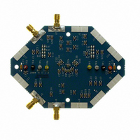
EVALUATION BOARD SCHEMATIC .1UF 1 1 C36 .1UF C37 .1UF C38 .1UF C39 .1UF C9 .1UF C10 .1UF 1 C11 .1UF C12 .1UF .1UF 1 C31 C43 .1UF .1UF C30 C42 .1UF .1UF C29 C41 .1UF ...
Page 14
... ADCLK907BCPZ-R7 −40°C to +125°C 1 ADCLK907BCPZ-R2 −40°C to +125°C 1 ADCLK925BCPZ-WP −40°C to +125°C ADCLK925BCPZ-R7 1 −40°C to +125°C 1 ADCLK925BCPZ-R2 −40°C to +125°C ADCLK905/PCBZ 1 1 ADCLK907/PCBZ 1 ADCLK925/PCBZ RoHS Compliant Part. 3.00 0.60 MAX BSC SQ 0. 2.75 TOP ...
Page 15
NOTES ADCLK905/ADCLK907/ADCLK925 Rev Page ...
Page 16
ADCLK905/ADCLK907/ADCLK925 NOTES ©2007 Analog Devices, Inc. All rights reserved. Trademarks and registered trademarks are the property of their respective owners. D06318-0-8/07(0) Rev Page ...