NB4N527SMNEVB ON Semiconductor, NB4N527SMNEVB Datasheet - Page 2
NB4N527SMNEVB
Manufacturer Part Number
NB4N527SMNEVB
Description
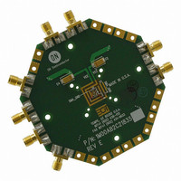
EVAL BOARD FOR NB4N527SMN
Manufacturer
ON Semiconductor
Datasheet
1.NB4N527SMNG.pdf
(10 pages)
Specifications of NB4N527SMNEVB
Main Purpose
Timing, Clock Buffer / Driver / Receiver / Translator
Embedded
No
Utilized Ic / Part
NB4N527S
Primary Attributes
Four Layer Board with Split (Dual) Power Supplies
Secondary Attributes
SMA Connectors
Silicon Manufacturer
On Semiconductor
Silicon Core Number
NB4N527S
Kit Application Type
Clock & Timing
Features
Temperature Compensated TIA/EIA644 Compliant LVDS Outputs
Lead Free Status / RoHS Status
Lead free / RoHS Compliant
Other names
NB4N527SMNEVBOS


1. In the differential configuration when the input termination pins(VTD0/VTD0, VTD1/ VTD1) are connected to a common termination voltage
Table 1. PIN DESCRIPTION
or left open, and if no signal is applied on D0/D0, D1/D1 input, then the device will be susceptible to self−oscillation.
6, 7
Pin
EP
10
11
12
13
14
15
16
1
2
3
4
5
8
9
Name
VTD1
VTD1
VTD0
VTD0
GND
V
NC
D1
D1
Q1
Q1
Q0
Q0
D0
D0
CC
LVCMOS, LVTTL, HSTL
LVCMOS, LVTTL, HSTL
LVCMOS, LVTTL, HSTL
LVCMOS, LVTTL, HSTL
LVPECL, CML, LVDS,
LVPECL, CML, LVDS,
LVPECL, CML, LVDS,
LVPECL, CML, LVDS,
LVDS Output
LVDS Output
LVDS Output
LVDS Output
I/O
V
V
−
−
−
−
−
TD1
TD1
D1
D1
Figure 3. Pin Configuration
1
2
3
4
VTD0 D0
GND NC
16
5
http://onsemi.com
NB4N527S
Internal 50 W termination pin for D1. (R
Noninverted differential clock/data D1 input (Note 1).
Inverted differential clock/data D1 input (Note 1).
Internal 50 W termination pin for D1. (R
0 V. Ground.
No connect.
Positive Supply Voltage.
Inverted D1 output. Typically loaded with 100 W receiver termination
resistor across differential pair.
Noninverted D1 output. Typically loaded with 100 W receiver termination
resistor across differential pair.
Inverted D0 output. Typically loaded with 100 W receiver termination
resistor across differential pair.
Noninverted D0 output. Typically loaded with 100 W receiver termination
resistor across differential pair.
Internal 50 W termination pin for D0.
Noninverted differential clock/data D0 input (Note 1).
Inverted differential clock/data D0 input (Note 1).
Internal 50 W termination pin for D0.
Exposed pad. EP on the package bottom is thermally connected to the die
improved heat transfer out of package. The pad is not electrically connected
to the die, but is recommended to be soldered to GND on the PCB.
NB4N527S
15
6
2
D0 VTD0
14
NC
7
13
V
8
CC
(Top View)
12
10
11
9
Q0
Q0
Q1
Q1
Exposed Pad (EP)
Description
TIN
TIN
)
)
Related parts for NB4N527SMNEVB
Image
Part Number
Description
Manufacturer
Datasheet
Request
R

Part Number:
Description:
3.3v, 2.5gb/s Dual Anylevel?? To Lvds Receiver/driver/buffer/translator With Internal Input Termination
Manufacturer:
ON Semiconductor
Datasheet:
Part Number:
Description:
ON Semiconductor [VOLTAGE REGULATOR]
Manufacturer:
ON Semiconductor
Datasheet:
Part Number:
Description:
357-036-542-201 CARDEDGE 36POS DL .156 BLK LOPRO
Manufacturer:
ON Semiconductor
Datasheet:
Part Number:
Description:
357-036-542-201 CARDEDGE 36POS DL .156 BLK LOPRO
Manufacturer:
ON Semiconductor
Datasheet:
Part Number:
Description:
357-036-542-201 CARDEDGE 36POS DL .156 BLK LOPRO
Manufacturer:
ON Semiconductor
Datasheet:
Part Number:
Description:
357-036-542-201 CARDEDGE 36POS DL .156 BLK LOPRO
Manufacturer:
ON Semiconductor
Datasheet:
Part Number:
Description:
357-036-542-201 CARDEDGE 36POS DL .156 BLK LOPRO
Manufacturer:
ON Semiconductor
Datasheet:
Part Number:
Description:
357-036-542-201 CARDEDGE 36POS DL .156 BLK LOPRO
Manufacturer:
ON Semiconductor
Datasheet:
Part Number:
Description:
357-036-542-201 CARDEDGE 36POS DL .156 BLK LOPRO
Manufacturer:
ON Semiconductor
Datasheet:
Part Number:
Description:
357-036-542-201 CARDEDGE 36POS DL .156 BLK LOPRO
Manufacturer:
ON Semiconductor
Datasheet:
Part Number:
Description:
357-036-542-201 CARDEDGE 36POS DL .156 BLK LOPRO
Manufacturer:
ON Semiconductor
Datasheet:
Part Number:
Description:
357-036-542-201 CARDEDGE 36POS DL .156 BLK LOPRO
Manufacturer:
ON Semiconductor
Datasheet:
Part Number:
Description:
Manufacturer:
ON Semiconductor
Datasheet:
Part Number:
Description:
Manufacturer:
ON Semiconductor
Datasheet: