AD5162EVAL Analog Devices Inc, AD5162EVAL Datasheet - Page 16
AD5162EVAL
Manufacturer Part Number
AD5162EVAL
Description
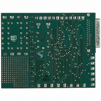
BOARD EVAL FOR AD5162
Manufacturer
Analog Devices Inc
Datasheet
1.AD5162BRMZ2.5.pdf
(20 pages)
Specifications of AD5162EVAL
Main Purpose
Digital Potentiometer
Utilized Ic / Part
AD5162
Lead Free Status / RoHS Status
Contains lead / RoHS non-compliant
Secondary Attributes
-
Embedded
-
Primary Attributes
-


AD5162
SPI INTERFACE
SPI-COMPATIBLE, 3-WIRE SERIAL BUS
The AD5162 contains a 3-wire, SPI-compatible digital interface
(SDI, CS , and CLK). The 9-bit serial word must be loaded MSB
first. The format of the word is shown in Table 8.
The positive-edge sensitive CLK input requires clean transitions
to avoid clocking incorrect data into the serial input register.
Standard logic families work well. If mechanical switches are
used for product evaluation, they should be debounced by a
flip-flop or another suitable means. When CS is low, the clock
loads data into the serial register on each positive clock edge
(see Figure 42).
The data setup and data hold times in Table 3 determine the
valid timing requirements. The AD5162 uses a 9-bit serial input
data register word that is transferred to the internal RDAC
register when the CS line returns to logic high. Extra MSB bits
are ignored.
(DATA IN)
V
CLK
OUT
SDI
CS
V
DD
1
0
1
0
1
0
0
Figure 43. SPI Interface Detailed Timing Diagram (V
t
CSH0
t
CSS
Dx
t
CH
Rev. C | Page 16 of 20
t
DS
Dx
t
CL
Table 8. Serial Data-Word Format
MSB
B8
A0
(2
1
The values of bits are shown in parentheses.
V
8
CLK
OUT
SDI
)
CS
t
CH
1
0
1
0
1
0
1
0
A
= 5 V, V
B7
D7
(2
t
CSH1
7
)
B
= 0 V, V
A0
Figure 42. SPI Interface Timing Diagram
B6
D6
t
CS1
D7
(V
W
t
S
t
= V
A
CSW
D6
= 5 V, V
B5
D5
OUT
)
D5
B
RDAC REGISTER LOAD
B4
D4
= 0 V, V
±1LSB
D4
D3
1
W
B3
D3
= V
D2
OUT
)
D1
B2
D2
D0
B1
D1
LSB
B0
D0
(2
0
)
Related parts for AD5162EVAL
Image
Part Number
Description
Manufacturer
Datasheet
Request
R


Part Number:
Description:
Board Mount Temperature Sensors TEMP MONITR DUAL CHN W/SERIES RSTNCE CNCL
Manufacturer:
ON Semiconductor
Datasheet:

Part Number:
Description:
Touch Screen Digitizer
Manufacturer:
Analog Devices, Inc.
Datasheet:
Part Number:
Description:
Half-duplex Icoupler-r Isolated Rs-485 Transceiver
Manufacturer:
Analog Devices, Inc.
Datasheet:

Part Number:
Description:
±1.7g Dual-Axis IMEMS Accelerometer Evaluation Board
Manufacturer:
Analog Devices Inc
Datasheet:

Part Number:
Description:
Inertial Sensor Evaluation System
Manufacturer:
Analog Devices Inc
Datasheet:
Part Number:
Description:
Manufacturer:
Analog Devices Inc
Datasheet:
Part Number:
Description:
Manufacturer:
Analog Devices Inc
Datasheet:
Part Number:
Description:
Manufacturer:
Analog Devices Inc
Datasheet:
Part Number:
Description:
Manufacturer:
Analog Devices Inc
Datasheet:
Part Number:
Description:
Manufacturer:
Analog Devices Inc
Datasheet: