ADNK-5023-SP02 Avago Technologies US Inc., ADNK-5023-SP02 Datasheet - Page 11
ADNK-5023-SP02
Manufacturer Part Number
ADNK-5023-SP02
Description
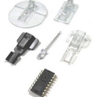
KIT REF DES OPTICAL MOUSE A5023
Manufacturer
Avago Technologies US Inc.
Datasheets
1.ADNK-5023-SP02.pdf
(24 pages)
2.ADNK-5023-SP02.pdf
(3 pages)
3.ADNK-5023-SP02.pdf
(10 pages)
Specifications of ADNK-5023-SP02
Main Purpose
Reference Design, Optical Mouse
Utilized Ic / Part
ADNS-5020
Description/function
Optical Mouse Sensor Kit
Interface Type
USB
Product
Display Modules
Touch Panel
No Touch Panel
For Use With/related Products
SPCP18A-13C
Lead Free Status / RoHS Status
Lead free / RoHS Compliant
Secondary Attributes
-
Embedded
-
Primary Attributes
-
Lead Free Status / Rohs Status
Details


NCS
SCLK
SDIO
SCLK
SDIO
LED Mode
For power savings, the LED will not be continuously on.
ADNS-5020-EN will pulse the LED only when needed.
Synchronous Serial Port
The synchronous serial port is used to set and read pa-
rameters in the ADNS-5020-EN, and to read out the
motion information.
The port is a three wire serial port. The host micro-con-
troller always initiates communication; the ADNS-5020-
EN never initiates data transfers. SCLK, SDIO, and NCS
may be driven directly by a micro-controller. The port
pins may be shared with other SPI slave devices. When
the NCS pin is high, the inputs are ignored and the
output is tri-stated.
The lines that comprise the SPI port:
SCLK:
SDIO:
NCS:
Write Operation
SDIO Setup and Hold Time
11
1/f
Clock input. It is always generated by the
master (the micro-controller).
Input and Output data.
Chip select input (active low). NCS needs to be
low to activate the serial port; otherwise, SDIO
will be high Z, and SDIO & SCLK will be ignored.
NCS can also be used to reset the serial port in
case of an error.
SCLK
t
setup
1
1/f
1
t
hold
SCLK
2
A 6
3
A 5
4
A 4
5
A 3
6
A 2
SDIO DRIVEN BY MICRO-CONTROLLER
7
A 1
8
A 0
9
D 7
Chip Select Operation
The serial port is activated after NCS goes low. If NCS
is raised during a transaction, the entire transaction
is aborted and the serial port will be reset. This is true
for all transactions. After a transaction is aborted, the
normal address-to-data or transaction-to-transaction
delay is still required before beginning the next trans-
action. To improve communication reliability, all serial
transactions should be framed by NCS. In other words,
the port should not remain enabled during periods of
non-use because ESD and EFT/B events could be inter-
preted as serial communication and put the chip into an
unknown state. In addition, NCS must be raised after
each burst-mode transaction is complete to terminate
burst-mode. The port is not available for further use until
burst-mode is terminated.
Write Operation
Write operation, defined as data going from the micro-
controller to the ADNS-5020-EN, is always initiated by
the micro-controller and consists of two bytes. The first
byte contains the address (seven bits) and has a “1” as its
MSB to indicate data direction. The second byte contains
the data. The ADNS-5020-EN reads SDIO on rising edges
of SCLK.
10
D 6
11
D 5
12
D 4
13
D 3
14
D 2
15
D 1
16
D 0
1
1
2
A 6
Related parts for ADNK-5023-SP02
Image
Part Number
Description
Manufacturer
Datasheet
Request
R

Part Number:
Description:
KIT SAMPLE FOR ADNS-5023
Manufacturer:
Avago Technologies US Inc.
Datasheet:

Part Number:
Description:
A2700 Sample Kit
Manufacturer:
Avago Technologies US Inc.
Datasheet:

Part Number:
Description:
OPTOCOUPLER GATE DRV 2A 16-SOIC
Manufacturer:
Avago Technologies US Inc.
Datasheet:
Part Number:
Description:
OPTOCOUPLER 2CH 2.5A 16-SOIC
Manufacturer:
Avago Technologies US Inc.
Datasheet:

Part Number:
Description:
OPTOCOUPLER GATE DRV 0.4A 16SOIC
Manufacturer:
Avago Technologies US Inc.
Datasheet:

Part Number:
Description:
OPTOCOUPLER 2.0A 250KHZ 8-DIP
Manufacturer:
Avago Technologies US Inc.
Datasheet:

Part Number:
Description:
OPTOCOUPLER 2.0A 250KHZ GW 8-SMD
Manufacturer:
Avago Technologies US Inc.
Datasheet:

Part Number:
Description:
OPTOCOUPLER 2CH 15MBD 3.3V 8SOIC
Manufacturer:
Avago Technologies US Inc.
Datasheet:
Part Number:
Description:
OPTOCOUPLER DARL-OUT 8-DIP
Manufacturer:
Avago Technologies US Inc.
Datasheet:
Part Number:
Description:
OPTOCOUPLER IGBT DRIVE 0.4A 8DIP
Manufacturer:
Avago Technologies US Inc.
Datasheet:
Part Number:
Description:
OPTOCOUPLER DARL-OUT 8-DIP
Manufacturer:
Avago Technologies US Inc.
Datasheet:

Part Number:
Description:
OPTOCOUPLER 1CH 1MBS 8-SMD GW
Manufacturer:
Avago Technologies US Inc.
Datasheet:
Part Number:
Description:
OPTOCOUPLER GATE DRIVER 8-DIP
Manufacturer:
Avago Technologies US Inc.
Datasheet:

Part Number:
Description:
OPTOCOUPLER GATE DRIVER 8-SMD
Manufacturer:
Avago Technologies US Inc.
Datasheet:

Part Number:
Description:
OPTOCOUPLER PHOTOTRANS 4-SMD
Manufacturer:
Avago Technologies US Inc.
Datasheet: