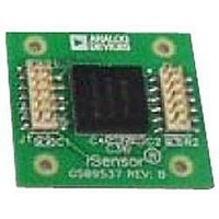
AD9122-M5375-EBZ Analog Devices Inc, AD9122-M5375-EBZ Datasheet - Page 58

AD9122-M5375-EBZ
Manufacturer Part Number
AD9122-M5375-EBZ
Description
BOARD EVALUATION AD9122
Manufacturer
Analog Devices Inc
Series
TxDAC+®r
Datasheet
1.AD9122BCPZRL.pdf
(60 pages)
Specifications of AD9122-M5375-EBZ
Number Of Adc's
2
Number Of Bits
16
Sampling Rate (per Second)
1.2G
Data Interface
Serial
Inputs Per Adc
1 Differential
Power (typ) @ Conditions
800mW @ 500MSPS
Operating Temperature
-40°C ~ 85°C
Utilized Ic / Part
AD9122, ADL5375
Silicon Manufacturer
Analog Devices
Application Sub Type
DAC
Kit Application Type
Data Converter
Silicon Core Number
AD9122
Lead Free Status / RoHS Status
Lead free / RoHS Compliant
AD9122
INTERFACE TIMING VALIDATION
The AD9122 provides on-chip sample error detection (SED)
circuitry that simplifies verification of the input data interface.
The SED compares the input data samples captured at the digital
input pins with a set of comparison values. The comparison values
are loaded into registers through the SPI port. Differences between
the captured values and the comparison values are detected and
stored. Options are available for customizing SED test sequencing
and error handling.
SED OPERATION
The SED circuitry operates on a data set made up of four 16-bit
input words, denoted as I0, Q0, I1, and Q1. To properly align
the input samples, the first I data-word (that is, I0 ) is indicated
by asserting FRAME for at least one complete input sample.
Figure 88 shows the input timing of the interface in word mode.
The FRAME signal can be issued once at the start of the data
transmission, or it can be asserted repeatedly at intervals coinciding
with the I0 and Q0 data-words.
The SED has three flag bits (Register 0x67, Bit 0, Bit 1, and
Bit 5) that indicate the results of the input sample comparisons.
The sample error detected bit (Register 0x67, Bit 5) is set when
an error is detected and remains set until cleared. The SED also
provides registers that indicate which input data bits experienced
errors (Register 0x70 through Register 0x73). These bits are
latched and indicate the accumulated errors detected until cleared.
The autoclear mode has two effects: it activates the compare fail
bit and the compare pass bit (Register 0x67, Bit 1 and Bit 0) and
changes the behavior of Register 0x70 through Register 0x73. The
compare pass bit sets if the last comparison indicated the
sample was error free. The compare fail bit sets if an error is
detected. The compare fail bit is automatically cleared by the
reception of eight consecutive error-free comparisons. When
autoclear mode is enabled, Register 0x70 through Register 0x73
accumulate errors as previously described but reset to all 0s after
eight consecutive error-free sample comparisons are made.
Table 27. Progression of Comparison Outcomes and the Resulting SED Register Values
Compare Results (Pass/Fail)
Register 0x67, Bit 5 (Sample Error Detected)
Register 0x67, Bit 1 (Compare Fail)
Register 0x67, Bit 0 (Compare Pass)
Register 0x70 to Register 0x73
1
2
DATA[15:0]
Z = all 0s.
N = nonzero.
Figure 88. Timing Diagram of Extended FRAME Signal Required to Align
(Errors Detected x_BITS[15:0])
FRAME
I0
Input Data for SED
Q0
I1
Q1
P
0
0
1
Z
I0
1
F
1
1
0
N
2
Q0
Rev. A | Page 58 of 60
F
N
1
1
0
2
F
1
1
0
N
2
P
1
1
1
N
The sample error, compare pass, and compare fail flags can be
configured to trigger an IRQ when active, if desired. This is
done by enabling the appropriate bits in the event flag register
(Register 0x07).
Table 27 shows a progression of the input sample comparison
results and the corresponding states of the error flags.
SED EXAMPLE
Normal Operation
The following example illustrates the SED configuration for
continuously monitoring the input data and assertion of an IRQ
when a single error is detected.
1.
2.
3.
If IRQ is asserted, read Register 0x67 and Register 0x70 through
Register 0x73 to verify that a SED error was detected and determine
which input bits were in error. The bits in Register 0x70 through
Register 0x73 are latched; therefore, the bits indicate any errors
that occurred on those bits throughout the test and not just the
errors that caused the error detected flag to be set.
Note that the FRAME signal is not required during normal
operation when the device is configured for word mode. To
enable the alignment of the I0 sample as described above
requires the use of the FRAME signal. The timing diagram for
byte and nibble modes are the same as during normal operation
and are shown in Figure 44 and Figure 45, respectively.
2
Write to the following registers to enable the SED and load
the comparison values:
Register 0x67 → 0x80
Register 0x68 → I0[7:0]
Register 0x69 → I0[15:8]
Register 0x6A → Q0[7:0]
Register 0x6B → Q0[15:8]
Register 0x6C → I1[7:0]
Register 0x6D → I1[15:8]
Register 0x6E → Q1[7:0]
Register 0x6F → Q1[15:8]
Comparison values can be chosen arbitrarily; however,
choosing values that require frequent bit toggling provides
the most robust test.
Enable the SED error detect flag to assert the IRQ pin.
Register 0x05 → 0x04
Begin transmitting the input data pattern.
P
1
1
1
N
2
P
1
1
1
N
2
P
1
1
1
N
2
P
1
1
1
N
2
P
1
1
1
N
2
P
1
1
1
N
2
P
1
1
1
N
2
P
1
0
1
Z
1
F
1
1
0
N
2
P
1
1
1
N
2
F
1
1
0
N
2


