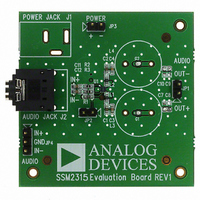
SSM2315-EVALZ Analog Devices Inc, SSM2315-EVALZ Datasheet
SSM2315-EVALZ
Specifications of SSM2315-EVALZ


Related parts for SSM2315-EVALZ


SSM2315-EVALZ Summary of contents
Page 1
... Input coupling capacitors can be omitted if the dc input common-mode voltage is approximately V The default gain of the SSM2315 is 6 dB, but users can reduce the gain by using a pair of external resistors (see the Gain section). The SSM2315 is specified over the industrial temperature range of − ...
Page 2
... SSM2315 TABLE OF CONTENTS Features .............................................................................................. 1 Applications ....................................................................................... 1 General Description ......................................................................... 1 Functional Block Diagram .............................................................. 1 Revision History ............................................................................... 2 Specifications ..................................................................................... 3 Absolute Maximum Ratings ............................................................ 4 Thermal Resistance ...................................................................... 4 ESD Caution .................................................................................. 4 Pin Configuration and Function Descriptions ............................. 5 Typical Performance Characteristics ............................................. 6 REVISION HISTORY 8/08—Rev Rev. A Changes to Efficiency and Total Harmonic Distortion + Noise Parameters ....................................................... 3 Changes to Ordering Guide .......................................................... 14 2/08— ...
Page 3
... NOISE PERFORMANCE Output Voltage Noise e Signal-to-Noise Ratio SNR 1 Note that although the SSM2315 has good audio quality above 3 W, continuous output power beyond 3 W must be avoided due to device packaging limitations. 2 This value represents measured performance; packaging limitations must not be exceeded. 1 Conditions Ω ...
Page 4
... SSM2315 ABSOLUTE MAXIMUM RATINGS Absolute maximum ratings apply at 25°C, unless otherwise noted. Table 2. Parameter Supply Voltage Input Voltage Common-Mode Input Voltage Continuous Output Power Storage Temperature Range Operating Temperature Range Junction Temperature Range Lead Temperature (Soldering, 60 sec) Stresses above those listed under Absolute Maximum Ratings may cause permanent damage to the device. This is a stress rating only ...
Page 5
... GND 3A OUT− 2B PVDD BALL A1 CORNER SSM2315 TOP VIEW BALL SIDE DOWN (Not to Scale) Figure 2. Pin Configuration Description Shutdown Input. Active low digital input. Ground. Noninverting Input. Inverting Input. Noninverting Output. Power Supply. Ground. Inverting Output. Power Supply. Rev Page SSM2315 ...
Page 6
... SSM2315 TYPICAL PERFORMANCE CHARACTERISTICS 100 R = 8Ω + 33µH L GAIN = 6dB 0.1 0.01 0.001 0.0001 0.001 0.01 0.1 OUTPUT POWER (W) Figure 3. THD + N vs. Output Power Ω μH, Gain = 100 R = 4Ω + 33µH L GAIN = 6dB 0.1 0.01 0.001 0.0001 0.001 0.01 0.1 OUTPUT POWER (W) Figure 4 ...
Page 7
... DD L 100 V = 2.5V DD GAIN = 6dB R = 4Ω + 33µ 0.5W 0.1 0.25W 0.125W 10 100 1k 10k FREQUENCY (Hz Ω μH, Gain = 100 V = 2.5V DD GAIN = 6dB R = 3Ω + 33µ 0.75W 1 0.1 0.375W 0.188W 10 100 1k 10k FREQUENCY (Hz Ω μH, Gain = SSM2315 100k 100k 100k ...
Page 8
... SSM2315 4.1 3.9 3 3Ω + 33µ 4Ω + 33µH L 3.3 NO LOAD 3.1 2.9 2.7 2.5 2.5 3.0 3.5 4.0 4.5 SUPPLY VOLTAGE (V) Figure 15. Supply Current vs. Supply Voltage 2.0 FREQUENCY = 1kHz GAIN = 6dB 1 8Ω + 33µH L 1.6 1.4 1.2 10% 1.0 0.8 0.6 ...
Page 9
... V Figure 25. Supply Current vs. Output Power 800 R 700 600 500 400 300 200 100 0 0.7 0.8 0 3.6 V Figure 26. Supply Current vs. Output Power Rev Page SSM2315 = 3. 4Ω + 33µH L 0.2 0.4 0.6 0.8 1.0 1.2 1.4 OUTPUT POWER ( Ω μ 8Ω + 33µ ...
Page 10
... SSM2315 0 –10 –20 –30 –40 –50 –60 –70 –80 –90 –100 10 100 1k FREQUENCY (Hz) Figure 27. Power Supply Rejection Ratio (PSRR) vs. Frequency 0 –10 –20 –30 –40 –50 –60 –70 –80 –90 –100 10 100 1k FREQUENCY (Hz) Figure 28. Common-Mode Rejection Ratio (CMRR) vs. Frequency –1 –2 10k 100k – ...
Page 11
... DRIVER IN– EXT 47nF 160kΩ SD INTERNAL BIAS OSCILLATOR Figure 32. Single-Ended Input Configuration, User-Adjustable Gain Rev Page VBATT 2.5V TO 5.5V VDD OUT+ FET OUT– POP/CLICK SUPPRESSION GND VBATT 2.5V TO 5.5V VDD OUT+ FET OUT– POP/CLICK SUPPRESSION GND SSM2315 ...
Page 12
... SSM2315 amplifiers. The SSM2315 also offers protection circuits for overcurrent and temperature protection. GAIN The SSM2315 has a default gain that can be reduced by using a pair of external resistors with a value calculated as follows: External Gain Settings = 160 kΩ/(80 kΩ POP-AND-CLICK SUPPRESSION Voltage transients at the output of audio amplifiers may occur when shutdown is activated or deactivated ...
Page 13
... ESL, low ESR capacitor, usually of around 4.7 μF. This capacitor bypasses low frequency noises to the ground plane. For high frequency transients noises, use a 0.1 μF capacitor as close as possible to the VDD pin of the device. Placing the decoupling capacitor as close as possible to the SSM2315 helps maintain efficient performance. Rev Page SSM2315 − ...
Page 14
... TOP VIEW (BALL SIDE DOWN) ORDERING GUIDE Model Temperature Range 1 SSM2315CBZ-R2 −40°C to +85°C SSM2315CBZ-REEL 1 −40°C to +85°C 1 SSM2315CBZ-REEL7 −40°C to +85°C 1 SSM2315-EVALZ RoHS Compliant Part. 0.655 0.600 0.545 SEATING PLANE 0.350 0.320 0.290 0.50 BALL PITCH 0.385 0.270 ...
Page 15
... NOTES Rev Page SSM2315 ...
Page 16
... SSM2315 NOTES ©2008 Analog Devices, Inc. All rights reserved. Trademarks and registered trademarks are the property of their respective owners. D06857-0-8/08(A) Rev Page ...