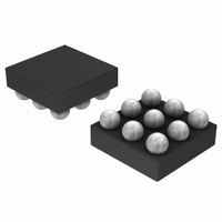
NCP2990FCT2GEVB ON Semiconductor, NCP2990FCT2GEVB Datasheet

NCP2990FCT2GEVB
Manufacturer Part Number
NCP2990FCT2GEVB
Description
EVAL BOARD FOR NCP2990FCT2G
Manufacturer
ON Semiconductor
Specifications of NCP2990FCT2GEVB
Design Resources
NCP2990 EVB BOM NCP2990FCT2GEVB Gerber Files NCP2990 EVB Schematic
Amplifier Type
Class AB
Output Type
1-Channel (Mono)
Max Output Power X Channels @ Load
1.35W x 1 @ 8 Ohm
Voltage - Supply
2.2 V ~ 5.5 V
Operating Temperature
-10°C ~ 75°C
Board Type
Fully Populated
Utilized Ic / Part
NCP2990
Lead Free Status / RoHS Status
Lead free / RoHS Compliant
For Use With/related Products
NCP2990FCT2G
Other names
NCP2990FCT2GEVBOS
09/13/2006
Output Power:
Quiescent Current:
Check the quiescent current. Place an 8 Ω load, no input signal. V
1. Set V
2. Set an 8 Ω load (resistance) on the output connector (J5).
3. With the function generator, set a single ended signal at 1 kHz and 0.5 Vrms input signal on the negative input. Apply this
4. Place 2 oscilloscope probes on the output (differential measurement). You should get a 1Vrms output signal with a “perfect
signal either on J2 or J3 connector. As R1=R2=20k, VO1 will see 0.5 Vrms. As VO1 signal is inverted by the second
amplifier, VO2 will also see 0.5 Vrms with 180° delay. Thus, the load between VO1 and VO2 will see 1 Vrms.
sine wave.” That is to say no clipping at the minima and maxima of the sine wave.
p
= 5 V to power supply connector (J1).
Test Procedure for the NCP2990EVB
p
set to 5 V and J6 closed. You should measure around 1.7 mA.