ADP1864-EVALZ Analog Devices Inc, ADP1864-EVALZ Datasheet - Page 11
ADP1864-EVALZ
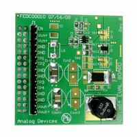
Manufacturer Part Number
ADP1864-EVALZ
Description
BOARD EVALUATION ADP1864
Manufacturer
Analog Devices Inc
Datasheets
1.ADP1864AUJZ-R7.pdf
(16 pages)
2.ADP1864-EVALZ.pdf
(12 pages)
3.ADP1864-BL-EVALZ.pdf
(16 pages)
Specifications of ADP1864-EVALZ
Main Purpose
DC/DC, Step Down
Outputs And Type
1, Non-Isolated
Voltage - Output
3.3V
Current - Output
3A
Voltage - Input
9 ~ 12V
Regulator Topology
Buck
Frequency - Switching
580kHz
Board Type
Fully Populated
Utilized Ic / Part
ADP1864
Silicon Manufacturer
Analog Devices
Application Sub Type
Step Down DC/DC Converter
Kit Application Type
Power Management - Voltage Regulator
Silicon Core Number
ADP1864
Kit Contents
Board
Lead Free Status / RoHS Status
Lead free / RoHS Compliant
Power - Output
-
Lead Free Status / RoHS Status
Lead free / RoHS Compliant, Lead free / RoHS Compliant


MOSFET
Choose the external P-channel MOSFET based on the following:
threshold voltage (V
R
The minimum operating voltage of the ADP1864 is 3.15 V.
Choose a MOSFET with a V
the minimum input supply voltage used in the application.
Ensure that the maximum ratings for MOSFET V
a few volts greater than the maximum input voltage used with
the ADP1864.
Estimate the rms current in the MOSFET under continuous
conduction mode by
Derate the MOSFET current by at least 20% to account for
inductor ripple and changes in the diode voltage.
The MOSFET power dissipation is the sum of the conducted
and switching losses:
where T = 0.005/°C × T
Ensure the maximum power dissipation calculated is significantly
less than the maximum rating of the MOSFET.
DIODE
The diode carries the inductor current during the off time of
the external FET. The average current of the diode is, therefore,
dependent on the duty cycle of the controller as well as the
output load current.
where V
A typical Schottky diode has a forward drop voltage of 0.5 V.
A Schottky diode is recommended for best efficiency because it
has a low forward drop and faster switching speed than junction
diodes. If a junction diode is used it must be an ultrafast recovery
diode. The low forward drop reduces power losses during the
FET off time, and fast switching speed reduces the switching
losses during PFET transitions.
DS(ON)
PD
I
I
DIODE
, and gate charge.
FET
FET(COND)
D
(
is the diode forward drop.
rms
(
AV
)
=
)
= 1
= (I
⎛
⎜
⎜
⎝
V
V
OUT
FET(rms)
−
T
IN
), maximum voltage and current ratings,
V
+
V
J (FET)
+
OUT
V
IN
)
V
2
D
D
× (1 + T) × R
+
+
T
− 25°C.
V
×
that is at least 1 V lower than
V
D
I
D
LOAD
⎞
⎟
⎟
⎠
×
I
LOAD
DS(ON)
SG
and V
SD
are
Rev. B | Page 11 of 16
(7)
(8)
(9)
INPUT CAPACITOR
The input capacitor provides a low impedance path for the
pulsed current drawn by the external P-channel FET. Choose
an input capacitor whose impedance at the switching frequency
is lower than the impedance of the voltage source (V
preferred input capacitor is a 10 μF ceramic capacitor due to
its low ESR and low impedance.
For all types of capacitors, make sure the ripple current rating
of the capacitor is greater than half of the maximum output
load current.
Where space is limited, multiple capacitors can be placed in
parallel to meet the rms current requirement. Place the input
capacitor as close as possible to the IN pin of the ADP1864.
OUTPUT CAPACITOR
The ESR and capacitance value of the output capacitor
determine the amount of output voltage ripple.
where f is the oscillator frequency (typically 580 kHz).
Because the output capacitance is typically >40 μF, the ESR
dominates the voltage ripple. Ensure the output capacitor
ripple rating is greater than the maximum inductor ripple.
POSCAP™ capacitors from Sanyo offer a good size, ESR, ripple,
and current capability trade-off.
FEEDBACK RESISTORS
The feedback resistors ratio sets the output voltage of the system.
Choose 80.6 kΩ for R2. Using higher values for R2 results in
reduced output voltage accuracy, and lower values cause an
increased voltage divider current, thus increasing quiescent
current consumption.
Δ
I
0
R1
rms
Figure 14. Two Feedback Resistors Used to Set Output Voltage
8 .
V
=
V
≅
≅
R2
Δ
=
2
I
V
×
×
×
1
OUT
(
⎛
⎜
⎜
⎝
V
3
8
OUT
R2
×
×
×
0
⎛
⎜
⎜
⎝
f
R1
8 .
(
−
V
×
1
R1
R
0
OUT
+
C
3
8 .
2
OUT
R
FB
)
ADP1864
2
+
L
V
+
×
D
ESR
) (
f
×
×
C
V
V
OUT
IN
IN
−
V
⎞
⎟
⎟
⎠
OUT
V
OUT
)
⎞
⎟
⎟
⎠
ADP1864
IN
). The
(10)
(11)
(12)
(13)
Related parts for ADP1864-EVALZ
Image
Part Number
Description
Manufacturer
Datasheet
Request
R

Part Number:
Description:
BOARD EVAL FOR ADP1864
Manufacturer:
Analog Devices Inc
Datasheet:
Part Number:
Description:
Blank Boards
Manufacturer:
Analog Devices Inc
Datasheet:

Part Number:
Description:
±1.7g Dual-Axis IMEMS Accelerometer Evaluation Board
Manufacturer:
Analog Devices Inc
Datasheet:
Part Number:
Description:
Inertial Sensor Evaluation System
Manufacturer:
Analog Devices Inc
Datasheet:
Part Number:
Description:
Manufacturer:
Analog Devices Inc
Datasheet:
Part Number:
Description:
Manufacturer:
Analog Devices Inc
Datasheet:
Part Number:
Description:
Manufacturer:
Analog Devices Inc
Datasheet:
Part Number:
Description:
Manufacturer:
Analog Devices Inc
Datasheet:
Part Number:
Description:
Manufacturer:
Analog Devices Inc
Datasheet:
Part Number:
Description:
Manufacturer:
Analog Devices Inc
Datasheet:
Part Number:
Description:
Manufacturer:
Analog Devices Inc
Datasheet:
Part Number:
Description:
Manufacturer:
Analog Devices Inc
Datasheet:
Part Number:
Description:
Manufacturer:
Analog Devices Inc
Datasheet: