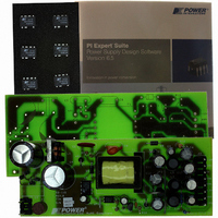
RDK-115 Power Integrations, RDK-115 Datasheet

RDK-115
Specifications of RDK-115
Related parts for RDK-115
RDK-115 Summary of contents
Page 1
TNY375-380 ® TinySwitch-PK Family Energy-Effi cient, Off-Line Switcher With Enhanced Peak Power Performance Product Highlights Lowest System Cost with Enhanced Flexibility Simple ON/OFF control, no loop compensation needed • Unique Peak Mode feature extends power range without • increasing transformer ...
Page 2
TNY375-380 BYPASS/ MULTI-FUNCTION (BP/M) LINE UNDER-VOLTAGE 115 μA 25 μA ENABLE JITTER 2X 1 OSCILLATOR ENABLE/ 1.0 V UNDER- VOLTAGE (EN/UV) 6.4 V Figure 2 Functional Block Diagram. Pin Functional Description DRAIN (D) Pin: This pin ...
Page 3
A modulation of the threshold current reduces group pulsing. The threshold current is between 75 μA and 115 μA. The EN/UV pin also senses line undervoltage conditions through an ...
Page 4
TNY375-380 BYPASS/MULTI-FUNCTION Pin Undervoltage The BYPASS/MULTI-FUNCTION pin undervoltage circuitry disables the power MOSFET when the BYPASS/MULTI- FUNCTION pin voltage drops below 4 steady state operation. Once the BYPASS/MULTI-FUNCTION pin voltage drops below 4 steady state operation, ...
Page 5
V EN CLOCK DC MAX I DRAIN V DRAIN Figure 6. Operation at Near Maximum Loading ( CLOCK DC MAX I DRAIN V DRAIN Figure 7. Operation at Moderately Heavy Loading (f Enable Function TinySwitch-PK senses the EN/UV ...
Page 6
TNY375-380 V EN CLOCK D MAX I DRAIN V DRAIN Figure 9. Operation at Very Light Load (f 132 kHz). OSC 200 V 100 DC-INPUT BYPASS 0 400 200 V DRAIN Time (ms) ...
Page 7
At very light loads, the current limit will be reduced even further (Figure 9). Only a small percentage of cycles will occur ...
Page 8
TNY375-380 D1 FR106 D2 F1 FR106 85-265 22 F VAC 400 1N4007 1N4007 TinySwitch-PK U1 TNY376P Figure 14. TNY376PN, Four Output, 7 ...
Page 9
Key Application considerations TinySwitch-PK Design Considerations Output Power Table Data sheet maximum output power table (Table 1) represents the maximum practical continuous output power level that can be obtained under the following assumed conditions: 1. The minimum DC input voltage ...
Page 10
TNY375-380 should be located as close as possible to the SOURCE and BYPASS pins of the device. For best performance of the OVP function recommended that a relatively high bias winding voltage is used, in the range of ...
Page 11
... TinySwitch-PK device as specifi the data sheet. Under low-line maximum power, a maximum TinySwitch-PK device SOURCE pin temperature of 110 °C is recommended to allow for these variations. Design Tools Up-to-date information on design tools can be found at the Power Integrations web site: www.powerint.com. TNY375-380 Maximize hatched copper areas ( ) for optimum heatsinking ...
Page 12
TNY375-380 (1,4) Absolute Maximum Ratings DRAIN Voltage .............................................................................. -0 700 V DRAIN Peak Current: TNY375 ...........................................................0.6 A TNY376 ...........................................................0.8 A TNY377 ........................................................... 1.4 A TNY378 ............................................................2.2 A TNY379 ...........................................................2.9 A TNY380...........................................................4.3 A EN/UV Voltage ................................................................................... -0 ...
Page 13
Parameter Symbol Control Functions (cont.) I CH1 BP/M Pin Charge Current I CH2 BP/M Pin Voltage V BP/M BP/M Pin Voltage V Hysteresis BP/MH BP/M Pin Shunt V Voltage SHUNT EN/UV Pin Line Under- I voltage Threshold LUV Circuit Protection ...
Page 14
TNY375-380 Parameter Symbol Circuit Protection (cont.) Peak Current Limit (BP/M Capacitor = I LIMITPEAKinc 10 μF) See Note E 2 Power Coeffi cient I f Initial Current Limit I INIT Leading Edge t Blanking Time LEB Current Limit Delay t ...
Page 15
Parameter Symbol Output ON-State R Resistance DS(ON) I DSS1 OFF-State Drain Leakage Current I DSS2 Breakdown BV Voltage DSS DRAIN Supply Voltage Auto-Restart t ON-Time OSC Auto-Restart DC Duty Cycle AR www.powerint.com Conditions SOURCE = 0 V; ...
Page 16
TNY375-380 NOTES: A. For all BP/M pin capacitor values accurate estimate of device controller current consumption at no-load, since operating frequency is so low under these S1 conditions. Total device consumption at no-load is the sum ...
Page 17
BP/M S EN/UV S NOTE: This test circuit is not applicable for current limit or output characteristic measurements. Figure 17. General Test Circuit. Figure 18. Duty Cycle Measurement. www.powerint.com 470 Ω 470 Ω ...
Page 18
TNY375-380 1.1 1.0 0.9 -50 - 100 125 150 Junction Temperature (°C) Figure 21. Breakdown vs. Temperature. 1.2 1 0.8 0.6 0.4 0 Temperature (°C) Figure 23. Standard Current Limit vs. Temperature. ...
Page 19
Scaling Factors: TNY375 1.0 120 TNY376 1.33 TNY377 2.33 TNY378 3.67 90 TNY379 4.87 TNY380 7. 200 DRAIN Voltage (V) Figure 27. Drain Capacitance Power. www.powerint.com 400 600 Figure 28. Undervoltage Threshold vs. Temperature. TNY375-380 ...
Page 20
TNY375-380 ⊕ .004 (.10) -E- .240 (6.10) .260 (6.60) Pin 1 .100 (2.54) (BSC) .367 (9.32) -D- .387 (9.83) .125 (3.18) .145 (3.68) .032 (.81) .048 (1.22) .037 (.94) .053 (1.35) ⊕ .004 (.10) -E- .240 ...
Page 21
B 4 4.90 (0.193) BSC A 8 3.90 (0.154) BSC 2 0.10 (0.004 Pin 1 ID 1.27 (0.050) BSC 1.25 - 1.65 1.35 (0.053) 1.75 (0.069) (0.049 - 0.065) 0.10 (0.004) 0.25 (0.010) Reference Solder Pad ...
Page 22
... The products and applications illustrated herein (including transformer construction and circuits external to the products) may be covered by one or more U.S. and foreign patents, or potentially by pending U.S. and foreign patent applications assigned to Power Integrations. A complete list of Power Integrations patents may be found at www.powerint.com. Power Integrations grants its customers a license under certain patent rights as set forth at http://www ...


