RDK-189 Power Integrations, RDK-189 Datasheet - Page 18
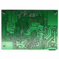
RDK-189
Manufacturer Part Number
RDK-189
Description
KIT REF DESIGN FOR PLC810
Manufacturer
Power Integrations
Series
HiperPLC™r
Specifications of RDK-189
Main Purpose
AC/DC, Primary Side
Outputs And Type
4, Isolated
Power - Output
225W
Voltage - Output
24V, 12V, 5V, 5V
Current - Output
7A, 4A, 1.9A, 100mA
Voltage - Input
90 ~ 265VAC
Regulator Topology
Flyback
Board Type
Fully Populated
Utilized Ic / Part
PLC810
Lead Free Status / RoHS Status
Lead free / RoHS Compliant
Frequency - Switching
-
Other names
596-1265


DC operating characteristics
Table 2 lists the minimum, typical, and maximum DC operating
voltages and currents for all inputs and outputs of PLC810PG.
Negative currents flow out of the IC, positive currents flow into
the IC. The DC operating characteristics are for a junction
Absolute Maximum Ratings
Table 1 lists the absolute maximum ratings. Stress beyond
these limits is likely to cause permanent damage to the
Table 1.
Rev. F 08/09
Absolute Maximum Ratings
Junction temperature ..................................... -40 °C to +125 °C
Storage temperature ...................................... -65 °C to +150 °C
Theta
Continuous supply voltage (VCC, VCCL)............... -0.3 V to 15 V
LLC voltage (HB pin) ........................................... -0.3 V to 600 V
LLC high side floating supply voltage
(VCCHB pin with respect to HB pin)...................... -0.3 V to V
Terminal Voltage With Respect To GND
3.3 V Tolerant pins ....................................... -0.3 V to V
ISL and ISP pins ........................................ -0.65 V to V
Power Supply Current
Startup Current
Inhibit Current
Operating Current
Leakage Current
Leakage Current
18
JA
Parameter
......................................................................... 35 °C/W
Absolute Maximum Ratings.
PLC810PG
Symbol
I
CCINHIBIT
I
I
CCOFF
CCON
I
I
OZ
OZ
(VCCL +
VCCHB)
ISP, ISL,
VCOMP,
FMAX
VCCL
VCCL
VCC
VCC
VCC
FBP,
Pin
ISP
PFC and LLC operating 100 kHz
/ 50% duty cycle, GATE outputs
VCC/VCCL/VCCHB = 12 V
unloaded, No Load on V
V(FBP) < INH (inhibit state)
REF
REF
0 < V
VCC/VCCL = UVLO -
+0.3 V
+0.3 V
VCC/VCCL = 12 V
CCL
IN
V
UVLO state.
VCCHB = 0
VCCHB = 0
IN
< V
Notes
= -0.48 V
LLC high side floating output voltage
(GATEH) ...................... .............................V
LLC low side output voltage (GATEL) ...........-0.3 V to VCCL+0.3
GNDP to GND ............. ........................................ -0.3 V to +0.3
GND to GNDL ............ ........................................ -0.3 V to +0.3
Power dissipation ..........................................................700 mW
ISL and ISP pins, max current....................................... -100 mA
I
REF
FMAX
temperature of -10 °C to 125 °C and VCC = 12 V, unless
otherwise noted. All voltages are relative to GNDP, GNDL or
GND (0 V). The pin names that are designated by VCC refer to
VCC, VCCL and VCCHB. The voltages on this pins are
respectively to GNDP/GND, GNDL and HB.
PLC810PG. Exposure to conditions above recommended
operating limits may effect performance and reliability. Normal
ESD handling precautions are recommended.
. Device in
............................. .................................................. 120 mA
REF
Min
-10
Typ
-10
1.1
0.7
1.1
3.0
60
7
HB
Max
-800
120
-0.3 to V
1.5
4.5
10
2
2
9
www.powerint.com
VCCHB
Units
mA
mA
mA
mA
mA
mA
+0.3
Related parts for RDK-189
Image
Part Number
Description
Manufacturer
Datasheet
Request
R

Part Number:
Description:
KIT REF DESIGN FOR LNK457D
Manufacturer:
Power Integrations
Datasheet:

Part Number:
Description:
REFERENCE DESIGN LINKSWITCH-PH
Manufacturer:
Power Integrations
Datasheet:

Part Number:
Description:
KIT REF DESIGN FOR LNK403EG
Manufacturer:
Power Integrations
Datasheet:

Part Number:
Description:
KIT REF DESIGN FOR LNK406EG
Manufacturer:
Power Integrations
Datasheet:

Part Number:
Description:
KIT REF DESIGN LINKSWITCH-CV
Manufacturer:
Power Integrations
Datasheet:

Part Number:
Description:
KIT REF DESIGN LINKSWITCH 2
Manufacturer:
Power Integrations
Datasheet:

Part Number:
Description:
Specifications: Family: Eval Boards - DC/DC & AC/DC (Off-Line) SMPS ; Series: HiperLCS™ ; Main Purpose: DC/DC, Step Down ; Outputs and Type: 1, Isolated ; Power - Output: 150W ; Voltage - Output: 24V ; Current - Output: 6.25A ; Voltage - Input:
Manufacturer:
Power Integrations, Inc.
Datasheet:

Part Number:
Description:
KIT DESIGN REF TINYSWITCH-III
Manufacturer:
Power Integrations
Datasheet:

Part Number:
Description:
KIT DESIGN REF LINKSWITCH LP
Manufacturer:
Power Integrations
Datasheet:

Part Number:
Description:
KIT REF DESIGN LED LINKSWITCH TN
Manufacturer:
Power Integrations
Datasheet:
Part Number:
Description:
KIT REF DESIGN PG LINKSWITCH-II
Manufacturer:
Power Integrations
Datasheet:
Part Number:
Description:
REFERENCE DESIGN LINKSWITCH-PL
Manufacturer:
Power Integrations
Datasheet:
Part Number:
Description:
REFERENCE DESIGN LINKSWITCH-PH
Manufacturer:
Power Integrations
Datasheet:

Part Number:
Description:
KIT REF DESIGN 36-72W MOTOR DRVR
Manufacturer:
Power Integrations
Datasheet:
Part Number:
Description:
Specifications: Manufacturer: Power Integrations ; Output Voltage: 380 VDC ; Input / Supply Voltage (Max): 264 VAC ; Input / Supply Voltage (Min): 90 VAC ; Mounting Style: Through Hole ; Output Current: 0.913 A ; Output Power: 347 W
Manufacturer:
Power Integrations, Inc.