NCP1207AADAPGEVB ON Semiconductor, NCP1207AADAPGEVB Datasheet - Page 9
NCP1207AADAPGEVB
Manufacturer Part Number
NCP1207AADAPGEVB
Description
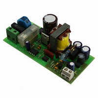
EVAL BOARD FOR NCP1207AADAPG
Manufacturer
ON Semiconductor
Datasheets
1.NCP1207APG.pdf
(17 pages)
2.NCP1207AADAPGEVB.pdf
(5 pages)
3.NCP1207AADAPGEVB.pdf
(8 pages)
Specifications of NCP1207AADAPGEVB
Design Resources
NCP1207AADAPGEVB BOM NCP1207AADAPGEVB Gerber Files NCP1207A EVB Schematic
Main Purpose
AC/DC, Primary Side
Outputs And Type
1, Isolated
Power - Output
24W
Voltage - Output
12V
Current - Output
2A
Voltage - Input
180 ~ 240VAC
Regulator Topology
Flyback
Frequency - Switching
70kHz
Board Type
Fully Populated
Utilized Ic / Part
NCP1207
Lead Free Status / RoHS Status
Lead free / RoHS Compliant
For Use With/related Products
NCP1207AADAPG
Other names
NCP1207AADAPGEVBOS


inserted between the current sense input and the sense element.
Every time the NCP1207A/B output driver goes low, a 200 mA
source forces a current to flow through the sense pin
(Figure 15): when the driver is high, the current source is off
and the current sense information is normally processed. As
soon as the driver goes low, the current source delivers 200 mA
and develops a ground referenced voltage across R
voltage is below the feedback voltage, the current sense
comparator stays in the high state and the internal latch can be
triggered by the next clock cycle. Now, if because of a low load
mode the feedback voltage is below R
RESET
The skip level selection is done through a simple resistor
Figure 15. A patented method allows for skip level
selection via a series resistor inserted in series
Figure 16. When the primary natural ringing becomes too low, the internal timeout together with the sense
Timeout
Timeout
+
--
Signal
Signal
Signal
Signal
Drain
Drain
with the current
+
3
2
DRIVER
comparator initiates a new cycle when FB passes the skip level.
DRIVER = HIGH ? I = 0
DRIVER = LOW ? I = 200 mA
R
skip
skip
level, then the
skip
R
sense
. If this
http://onsemi.com
5 ms
Current Sense and Timeout Re--start
Demag Re--start
9
current sense comparator permanently resets the latch and the
next clock cycle (given by the demagnetization detection) is
ignored: we are skipping cycles as shown by Figure 16. As
soon as the feedback voltage goes up again, there can be two
situations: the recurrent period is small and a new
demagnetization detection (next wave) signal triggers the
NCP1207A/B. To the opposite, in low output power
conditions, no more ringing waves are present on the drain and
the toggling of the current sense comparator together with the
internal 5 ms timeout initiates a new cycle start. In normal
operating conditions, e.g. when the drain oscillations are
generous, the demagnetization comparator can detect the
50 mV crossing and gives the “green light”, alone, to re- -active
the power switch. However, when skip cycle takes place (e.g.
at low output power demands), the re- -start event slides along
the drain ringing waveforms (actually the valley locations)
which decays more or less quickly, depending on the
L
thus quickly occur where the ringing becomes too weak to be
detected by the demagnetization comparator: it then
permanently stays locked in a given position and can no longer
deliver the “green light” to the controller. To help in this
situation, the NCP1207A/B implements a 5 ms timeout
generator: each time the 50 mV crossing occurs, the timeout is
reset. So, as long as the ringing becomes too low, the timeout
generator starts to count and after 5 ms, it delivers its “green
light”. If the skip signal is already present then the controller
re- -starts; otherwise the logic waits for it to set the drive output
high. Figure 16 depicts these two different situations:
primary
- -C
parasitic
5 ms
network damping factor. The situation can
Related parts for NCP1207AADAPGEVB
Image
Part Number
Description
Manufacturer
Datasheet
Request
R

Part Number:
Description:
PWM Current-Mode Controller for Free Running Quasi-Resonant Operation
Manufacturer:
ON

Part Number:
Description:
ON Semiconductor [VOLTAGE REGULATOR]
Manufacturer:
ON Semiconductor
Datasheet:
Part Number:
Description:
357-036-542-201 CARDEDGE 36POS DL .156 BLK LOPRO
Manufacturer:
ON Semiconductor
Datasheet:
Part Number:
Description:
357-036-542-201 CARDEDGE 36POS DL .156 BLK LOPRO
Manufacturer:
ON Semiconductor
Datasheet:
Part Number:
Description:
357-036-542-201 CARDEDGE 36POS DL .156 BLK LOPRO
Manufacturer:
ON Semiconductor
Datasheet:
Part Number:
Description:
357-036-542-201 CARDEDGE 36POS DL .156 BLK LOPRO
Manufacturer:
ON Semiconductor
Datasheet:
Part Number:
Description:
357-036-542-201 CARDEDGE 36POS DL .156 BLK LOPRO
Manufacturer:
ON Semiconductor
Datasheet:
Part Number:
Description:
357-036-542-201 CARDEDGE 36POS DL .156 BLK LOPRO
Manufacturer:
ON Semiconductor
Datasheet:
Part Number:
Description:
357-036-542-201 CARDEDGE 36POS DL .156 BLK LOPRO
Manufacturer:
ON Semiconductor
Datasheet:
Part Number:
Description:
357-036-542-201 CARDEDGE 36POS DL .156 BLK LOPRO
Manufacturer:
ON Semiconductor
Datasheet:
Part Number:
Description:
357-036-542-201 CARDEDGE 36POS DL .156 BLK LOPRO
Manufacturer:
ON Semiconductor
Datasheet:
Part Number:
Description:
357-036-542-201 CARDEDGE 36POS DL .156 BLK LOPRO
Manufacturer:
ON Semiconductor
Datasheet:
Part Number:
Description:
Manufacturer:
ON Semiconductor
Datasheet:
Part Number:
Description:
Manufacturer:
ON Semiconductor
Datasheet: