STEVAL-ISA039V1 STMicroelectronics, STEVAL-ISA039V1 Datasheet
STEVAL-ISA039V1
Specifications of STEVAL-ISA039V1
Available stocks


Related parts for STEVAL-ISA039V1


STEVAL-ISA039V1 Summary of contents
Page 1
Feature ■ Flexible power supply from ■ Power conversion input as low as 1.5 V ■ output voltage accuracy ■ High-current integrated drivers ■ Adjustable output voltage ■ 0.8 V internal reference ■ ...
Page 2
Contents Contents 1 Typical application circuit and block diagram . . . . . . . . . . . . . . . . . . . . 4 1.1 Application circuit . . . . . . . ...
Page 3
L6727 9.3 Layout guidelines . . . . . . . . . . . . . . . . . . . . . . . . . . . . . . . . . . . . ...
Page 4
Typical application circuit and block diagram 1 Typical application circuit and block diagram 1.1 Application circuit Figure 1. Typical application circuit 12V CC C DEC 1.2 Block diagram Figure 2. Block diagram ...
Page 5
L6727 2 Pins description and connection diagrams Figure 3. Pins connection (top view) 2.1 Pin descriptions Table 2. Pins descriptions Pin # Name 1 BOOT 2 UGATE 3 GND 4 LGATE 5 VCC 6 FB COMP / DIS 7 / ...
Page 6
Electrical specifications 2.2 Thermal data Table 3. Thermal data Symbol R Thermal resistance junction to ambient thJA T Maximum junction temperature MAX T Storage temperature range STG T Junction temperature range J 1. Measured with the component mounted on a ...
Page 7
L6727 3.2 Electrical characteristics = -20 °C to +85 °C, unless otherwise specified Table 5. Electrical characteristics Symbol Parameter Recommended operating conditions V Device supply voltage CC V Conversion input voltage IN Supply ...
Page 8
Electrical specifications Table 5. Electrical characteristics (continued) Symbol Parameter V OC Switch-over threshold CC_OC V Fixed OC threshold OCTH Over and undervoltage protections OVP OVP threshold UVP UVP threshold 1. Guaranteed by design, not subject to test. 8/34 Test conditions ...
Page 9
L6727 4 Device description L6727 is a single-phase PWM controller with embedded high-current drivers that provides complete control logic and protections to realize in an easy and simple way a general DC- DC step-down converter. Designed to drive N-channel MOSFETs ...
Page 10
Driver section 5 Driver section The integrated high-current drivers allow using different types of power MOSFET (also multiple MOSFETs to reduce the equivalent R The driver for the high-side MOSFET uses BOOT pin for supply and PHASE pin for return. ...
Page 11
L6727 6 Soft-start and disable L6727 implements a soft-start to smoothly charge the output filter avoiding high in-rush currents to be required from the input power supply. The device progressively increases the internal reference from 0.8 V ...
Page 12
Soft-start and disable 6.2 Enable / disable The device can be disabled by externally pushing COMP / DIS pin under 0.5 V (typ). In disable condition HS and LS MOSFETs are turned off, and a 20 μA current is sourced ...
Page 13
L6727 7 Overcurrent protection The overcurrent feature protects the converter from a shorted output or overload, by sensing the output current information across the low side MOSFET drain-source on-resistance This method reduces cost and enhances converter efficiency by ...
Page 14
Output voltage monitor and protections 8 Output voltage monitor and protections L6727 monitors the voltage at FB pin and compares it to internal reference voltage in order to provide Under Voltage and Over Voltage protections. 8.1 Undervoltage protection If the ...
Page 15
L6727 9 Application details 9.1 Output voltage selection L6727 is capable to precisely regulate an output voltage as low as 0 fact, the device comes with a fixed 0.8 V internal reference that guarantees the output regulated voltage ...
Page 16
Application details Compensation goal is to close the control loop assuring high DC regulation accuracy, good dynamic performances and stability. To achieve this, the overall loop needs high DC gain, high bandwidth and good phase margin. High DC gain is ...
Page 17
L6727 To place the poles and zeroes of the compensation network, the following suggestions may be followed: a) Set the gain R according to the approximated formula (suggested values for kΩ): R F ---------- ...
Page 18
Application details same high-current trace on more than one PCB layer will reduce the parasitic resistance associated to that connection. Connect output bulk capacitors (C inductance and resistance associated to the copper trace, also adding extra decoupling capacitors along the ...
Page 19
L6727 9.4 Embedding L6727-based VRs When embedding the VR into the application, additional care must be taken since the whole switching DC/DC regulator and the most common system in which it has to work is a digital ...
Page 20
Application information 10 Application information 10.1 Output inductor Inductor value is defined by a compromise between dynamic response, ripple, efficiency, cost and size. Usually, inductance is calculated to maintain inductor ripple current (ΔI between 20 % and ...
Page 21
L6727 10.2 Output capacitors Output capacitors choice depends on the application constraints in point of output voltage ripple and output voltage deviation during a load transient. During steady-state conditions, the output voltage ripple is influenced by ESR and capacitance of ...
Page 22
A demonstration board demonstration board L6727 demonstration board realizes on a four-layer PCB a step-down DC/DC converter and shows the operation of the device in a general purpose application. Input voltage can range from 5 V ...
Page 23
L6727 Figure 13 demonstration board inner layers Doc ID 12933 Rev demonstration board 23/34 ...
Page 24
A demonstration board Figure 14 demonstration board schematic PHASE PHASE HSD 24/34 GND GND PHASE ...
Page 25
L6727 Table demonstration board - bill of material Qty Capacitors 2 C1 C10 3 C11 to C13 2 C14, C38 2 C18, C25 1 C23 1 C24 1 C35 Resistors 2 R1 R17 ...
Page 26
A demonstration board 11.1 Board description 11.1.1 Power input (VIN) This is the input voltage for the power conversion. The high-side MOSFET drain is connected to this input. Supply must be compliant with VIN recommended operating conditions and capacitors ...
Page 27
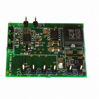
L6727 demonstration board L6727 demonstration board realizes on a two-layer PCB a step-down DC/DC converter and shows the operation of the device in a general-purpose low-current application. Input voltage can range from ...
Page 28
A demonstration board Figure 18 demonstration board schematic 28/34 L6727 L6727 GND Doc ID 12933 Rev 4 L6727 OUT OUT OUT OUT OUT OUT OUT OUT OUT OUT OUT OUT OUT OUT OUT OUT ...
Page 29
L6727 Table demonstration board - bill of material Qty Capacitors 2 C12, C51 1 C10 2 C14, C38 1 C39 1 C30 2 C23, C36 1 C24 1 C35 Resistors R3, R5, R8, R16 ...
Page 30
A demonstration board 12.1 Board description 12.1.1 Power input (VIN) This is the input voltage for the power conversion. The high-side MOSFET drain is connected to this input. Supply must be compliant with VIN recommended operating conditions and capacitors ...
Page 31
L6727 13 Package mechanical data In order to meet environmental requirements, ST offers these devices in different grades of ® ECOPACK packages, depending on their level of environmental compliance. ECOPACK specifications, grade definitions and product status are available at: www.st.com. ...
Page 32
Package mechanical data Figure 20. Package dimensions 32/34 Doc ID 12933 Rev 4 L6727 ...
Page 33
L6727 14 Revision history Table 9. Revision history Date 04-Dec-2006 28-Feb-2007 06-Jun-2007 23-Mar-2010 Revision 1 Initial release. 2 Updated V values in OCTH Updated Figure 1: Typical application circuit on page 3 Table 3 and Table 4 on page 6 ...
Page 34
... Information in this document is provided solely in connection with ST products. STMicroelectronics NV and its subsidiaries (“ST”) reserve the right to make changes, corrections, modifications or improvements, to this document, and the products and services described herein at any time, without notice. All ST products are sold pursuant to ST’s terms and conditions of sale. ...