IRDC3640 International Rectifier, IRDC3640 Datasheet
IRDC3640
Specifications of IRDC3640


Related parts for IRDC3640

IRDC3640 Summary of contents
Page 1
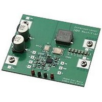
... MOSFET performance. This user guide contains the schematic and bill of materials for the IR3640 evaluation board. The guide describes operation and use of the evaluation board itself. Detailed , information for IR3640 is available in the IR3640 data sheet. IRDC3640 for optimum cost and application 1 ...
Page 2
... IR3640. To improve efficiency, the circuit board is designed to minimize the length of the on-board power ground current path. Table I. Connections Signal Name V (+12V) in Ground Vcc input Ground for Vcc input V (+1.8V) out Ground of Vout Synchronous input Power Good Signal IRDC3640 2 ...
Page 3
... Connection Diagram V = +12V in GROUND Fig. 1: Connection diagram of IR3640 evaluation board (top and bottom) GROUND Vcc = +5V IRDC3640 V = +1.8V OUT GROUND 3 ...
Page 4
... Fig. 2: Board layout, top layer Fig. 3: Board layout, bottom layer IRDC3640 4 ...
Page 5
... Single point connection between AGND and PGND. Fig. 4: Board layout, mid-layer I Fig. 5: Board layout, mid-layer II IRDC3640 5 ...
Page 6
... Fig. 6: Board layout, mid-layer III Fig. 7: Board layout, mid-layer IV IRDC3640 6 ...
Page 7
... Boot 7 NC1 1 Comp NC6 6 Sync Enable LGnd 1 8 PVcc IRDC3640 ...
Page 8
... Thick-film,0603,1/10 W,1% 4.12K Thick-film,0603,1/10 W,1% 3.24K Thick-film,0603,1/10W,1% 130 Thick-film,0603,1/10 W,1% 4.02K Thick-film,0603,1/10 W,1% 20 Thick-film,0603,1/10 W,1% Label TP 0.250" x 0.300" test pad area IR3640 IR3640,Controller,MLPQ,3x4mm IRDC3640 Manufacturer Part Number Taiyo-Yuden TMK325BJ106MN-T Panasonic ECJ-1VB1H104K Murata Electronics GRM21BR60G476ME15L Murata Electronics GRM188R61E105KA12D Panasonic-ECG C1608C0G1E562J Murata Electronics GRM1885C1H161JA01D ...
Page 9
... Vin=12.0V, Vcc=5V, Vo=1.8V, Io=0- 25A, Room Temperature, No Air Flow Fig. 9: Start Load (Note :PGood Fig. 11: Start up with 1.5V Prebias, 0A Load out 3 SS Fig. 13: Inductor node at 25A load Ch : PGood 4 IRDC3640 Fig. 10: Start up at 25A Load (Note :PGood Fig. 12: Output Voltage Ripple, 25A load out Fig. 14: Short (Hiccup) Recovery :Io 2 out ...
Page 10
... TYPICAL OPERATING WAVEFORMS Vin=12V, Vcc=5V, Vo=1.8V, Room Temperature, No Air Flow Note1: Enable is tied to Vin via a resistor divider and triggered when Vin is exceeding above 10V. Fig. 15: Transient Response 0A-12.5A load out 4 o IRDC3640 10 ...
Page 11
... TYPICAL OPERATING WAVEFORMS Vin=12V, Vcc=5V, Vo=1.8V, Io=0-25A, Room Temperature, No Air Flow Fig.16: Bode Plot at 25A load shows a bandwidth of 113.6kHz and phase margin of 50.4 degrees IRDC3640 11 ...
Page 12
... TYPICAL OPERATING WAVEFORMS Vin=12V, Vo=1.8V, Io=0-25A, Room Temperature, No Air Flow IR3640_IRF6710_IRF6795_0.33uH Efficiency vs IR3640_IRF6710_IRF6795_0.33uH Power Loss vs Fig.17: Efficiency and power loss vs. load current Io( Io(A) IRDC3640 ...
Page 13
... THERMAL IMAGES Vin=12V, Vo=1.8V, Io=25A, Room Temperature, No Air Flow Test Point 1: Ctrl FET IRF6710, Test Point 2: Sync FET IRF6795 2 Fig.18: Thermal Image at 25A load Test Point 3: Inductor IRDC3640 13 ...
Page 14
... However, the minimum metal to metal spacing should be ≥ 0.17mm for 2 oz. Copper (≥ 0.1mm for 1 oz. Copper and ≥ 0.23mm for 3 oz. Copper). Four 0.30mm diameter via shall be placed in the center of the pad land and connected to ground to minimize the noise effect on the IC. IRDC3640 ...
Page 15
... Ensure that the solder resist in-between the lead lands and the pad land is ≥ 0.15mm due to the high aspect ratio of the solder resist strip separating the lead lands from the pad land. Each via in the land pad should be tented or plugged from bottom boardside with solder resist. IRDC3640 ...
Page 16
... The maximum length and width of the land pad stencil aperture should be equal to the solder resist opening minus an annular 0.2mm pull back to decrease the incidence of shorting the center land to the lead lands when the part is pushed into the solder paste. IRDC3640 ...
Page 17
... This product has been designed and qualified for the Consumer market. Data and specifications subject to change without notice. 11/07 233 Kansas St., El Segundo, California 90245, USA Tel: (310) 252-7105 Visit us at www.irf.com for sales contact information IRDC3640 TAC Fax: (310) 252-7903 ...