AD9117-EBZ Analog Devices Inc, AD9117-EBZ Datasheet - Page 47
AD9117-EBZ
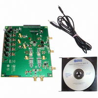
Manufacturer Part Number
AD9117-EBZ
Description
BOARD EVALUATION FOR AD9117
Manufacturer
Analog Devices Inc
Series
TxDAC®r
Datasheet
1.AD9114BCPZ.pdf
(80 pages)
Specifications of AD9117-EBZ
Number Of Dac's
2
Number Of Bits
14
Outputs And Type
2, Differential
Sampling Rate (per Second)
125M
Data Interface
Serial
Dac Type
Current
Voltage Supply Source
Analog and Digital
Operating Temperature
-40°C ~ 85°C
Utilized Ic / Part
AD9117
Lead Free Status / RoHS Status
Lead free / RoHS Compliant


APPLICATIONS INFORMATION
OUTPUT CONFIGURATIONS
The following sections illustrate some typical output configu-
rations for the AD9114/AD9115/AD9116/AD9117. Unless
otherwise noted, it is assumed that I
20 mA. For applications requiring the optimum dynamic
performance, a differential output configuration is suggested.
A differential output configuration can consist of either an RF
transformer or a differential op amp configuration. The trans-
former configuration provides the optimum high frequency
performance and is recommended for any application that
allows ac coupling. The differential op amp configuration is
suitable for applications requiring dc coupling, signal gain,
and/or a low output impedance.
A single-ended output is suitable for applications in which low
cost and low power consumption are primary concerns.
DIFFERENTIAL COUPLING USING A TRANSFORMER
An RF transformer can be used to perform a differential-to-
single-ended signal conversion, as shown in Figure 102. The
distortion performance of a transformer typically exceeds
that available from standard op amps, particularly at higher
frequencies. Transformer coupling provides excellent rejection
of common-mode distortion (that is, even-order harmonics)
over a wide frequency range. It also provides electrical isolation
and can deliver voltage gain without adding noise. Transformers
with different impedance ratios can also be used for impedance
matching purposes. The main disadvantages of transformer
coupling are low frequency roll-off, lack of power gain, and
high output impedance.
The center tap on the primary side of the transformer must be
connected to a voltage that keeps the voltages on IOUTP and
IOUTN within the output common-mode voltage range of the
device. Note that the dc component of the DAC output current
is equal to I
The center tap of the transformer should provide a path for this
dc current. In most applications, AGND provides the most
convenient voltage for the transformer center tap. The comple-
mentary voltages appearing at IOUTP and IOUTN (that is,
V
should be maintained with the specified output compliance
range of the AD9114/AD9115/AD9116/AD9117.
IOUTP
AD9114/AD9115/
AD9116/AD9117
and V
Figure 102. Differential Output Using a Transformer
IOUTFS
IOUTN
IOUTN
IOUTP
and flows out of both IOUTP and IOUTN.
) swing symmetrically around AGND and
29
28
OPTIONAL R
xOUTFS
is set to a nominal
DIFF
R
LOAD
Rev. A | Page 47 of 80
A differential resistor, R
which the output of the transformer is connected to the load,
R
reflected by the transformer, is chosen to provide a source
termination that results in a low voltage standing wave ratio
(VSWR). Note that approximately half the signal power is
dissipated across R
SINGLE-ENDED BUFFERED OUTPUT USING
AN OP AMP
An op amp, such as the ADA4899-1, can be used to perform a single-
ended current-to-voltage conversion, as shown in Figure 103. The
AD9114/AD9115/AD9116/AD9117 are configured with a pair of
series resistors, R
R
the peak-to-peak signal swing by the formula
The common-mode voltage of the output is determined by the
formula
The maximum and minimum voltages out of the amplifier are,
respectively,
LOAD
S
should be set to 0 Ω. The feedback resistor, R
AD9114/AD9115/
AD9116/AD9117
V
V
V
V
, via a passive reconstruction filter or cable. R
OUT
MIN
CM
MAX
= V
= R
=
=
AD9114/AD9115/AD9116/AD9117
V
Figure 103. Single-Supply, Single-Ended Buffer
V
REF
FB
MAX
REF
IOUTP
IOUTN
REFIO
AVSS
× I
S
×
, off each output. For best distortion performance,
− I
×
⎛
⎜
⎜
⎝
FS
DIFF
1
⎛
⎜
⎜
⎝
FS
28
34
29
25
1
+
.
+
× R
R
R
DIFF
R
FB
R
B
R
FB
FB
B
S
, can be inserted in applications in
⎞
⎟
⎟
⎠
R
⎞
⎟
⎟
⎠
−
S
R
FB
R
C
B
2
×
I
FS
ADA4899-1
–
+
+5V
–5V
R
C
FB
F
FB
, determines
DIFF
, as
V
OUT
Related parts for AD9117-EBZ
Image
Part Number
Description
Manufacturer
Datasheet
Request
R

Part Number:
Description:
Dual 14B, Low Power D-A Converter
Manufacturer:
Analog Devices Inc
Datasheet:

Part Number:
Description:
±1.7g Dual-Axis IMEMS Accelerometer Evaluation Board
Manufacturer:
Analog Devices Inc
Datasheet:
Part Number:
Description:
Inertial Sensor Evaluation System
Manufacturer:
Analog Devices Inc
Datasheet:
Part Number:
Description:
Manufacturer:
Analog Devices Inc
Datasheet:
Part Number:
Description:
Manufacturer:
Analog Devices Inc
Datasheet:
Part Number:
Description:
Manufacturer:
Analog Devices Inc
Datasheet:
Part Number:
Description:
Manufacturer:
Analog Devices Inc
Datasheet:
Part Number:
Description:
Manufacturer:
Analog Devices Inc
Datasheet:
Part Number:
Description:
Manufacturer:
Analog Devices Inc
Datasheet:
Part Number:
Description:
Manufacturer:
Analog Devices Inc
Datasheet:
Part Number:
Description:
Manufacturer:
Analog Devices Inc
Datasheet:
Part Number:
Description:
Manufacturer:
Analog Devices Inc
Datasheet:
Part Number:
Description:
Manufacturer:
Analog Devices Inc
Datasheet: