CDB4351 Cirrus Logic Inc, CDB4351 Datasheet
CDB4351
Specifications of CDB4351


Related parts for CDB4351


CDB4351 Summary of contents
Page 1
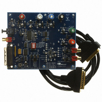
... The CS4351 is available in a 20-pin TSSOP package in both Commercial (-10°C - +70°C) and Automotive grades (-40°C to +85°C). The CDB4351 Customer Demonstration board is also available for device evalu- ation and implementation suggestions. Please see “Ordering Information” on page 37 ...
Page 2
TABLE OF CONTENTS 1. PIN DESCRIPTION ............................................................................................................................... 5 2. CHARACTERISTICS AND SPECIFICATIONS ..................................................................................... 6 SPECIFIED OPERATING CONDITIONS .............................................................................................. 6 ABSOLUTE MAXIMUM RATINGS ........................................................................................................ 6 DAC ANALOG CHARACTERISTICS .................................................................................................... 7 COMBINED INTERPOLATION & ON-CHIP ANALOG FILTER RESPONSE ....................................... 8 COMBINED INTERPOLATION ...
Page 3
ATAPI Channel Mixing and Muting (ATAPI3:0) Bits 3-0 .................................................. 26 6.4 Mute Control - Register 04h ........................................................................................................ 27 6.4.1 Auto-Mute (AMUTE) Bit 7 ................................................................................................ 27 6.4.2 AMUTEC = BMUTEC (MUTEC A=B) Bit 5 ...................................................................... 27 6.4.3 A Channel Mute ...
Page 4
Figure 29.Quad-Speed (fast) Stopband Rejection ..................................................................................... 33 Figure 30.Quad-Speed (fast) Transition Band ........................................................................................... 33 Figure 31.Quad-Speed (fast) Transition Band (detail) ............................................................................... 34 Figure 32.Quad-Speed (fast) Passband Ripple ......................................................................................... 34 Figure 33.Quad-Speed (slow) Stopband Rejection.................................................................................... 34 Figure 34.Quad-Speed (slow) Transition Band.......................................................................................... ...
Page 5
PIN DESCRIPTION MCLK DIF1(SCL/CCLK) DIF0(SDA/CDIN) DEM(AD0/CS) Pin Name # SDIN 1 Serial Audio Data Input (Input) - Input for two’s complement serial audio data. SCLK 2 Serial Clock (Input) - Serial clock for the serial audio interface. Left / ...
Page 6
CHARACTERISTICS AND SPECIFICATIONS (Min/Max performance characteristics and specifications are guaranteed over the Specified Operating Conditions. Typical specifications are derived from performance measurements 3.3 V.) SPECIFIED OPERATING CONDITIONS (GND = 0 V; all voltages with respect ...
Page 7
DAC ANALOG CHARACTERISTICS (Test conditions (unless otherwise specified): input test signal is a 997 Hz sine wave at 0 dBFS; measurement bandwidth kHz) Parameter All Speed Modes Fs = 48, 96, and 192 kHz Dynamic Range ...
Page 8
COMBINED INTERPOLATION & ON-CHIP ANALOG FILTER RESPONSE (The filter characteristics have been normalized to the sample rate (Fs) and can be referenced to the desired sam- ple rate by multiplying the given characteristic by Fs. See Parameter Combined Digital and ...
Page 9
COMBINED INTERPOLATION & ON-CHIP ANALOG FILTER RESPONSE (Continued) Parameter Single-Speed Mode - 48 kHz Passband (Note 3) Frequency Response kHz StopBand StopBand Attenuation Total Group Delay (Fs = Output Sample Rate) Intra-channel Phase Deviation Inter-channel Phase ...
Page 10
SWITCHING SPECIFICATIONS - SERIAL AUDIO INTERFACE Parameters MCLK Frequency MCLK Duty Cycle Input Sample Rate (Manual selection) Quad-Speed Mode Input Sample Rate (Auto selection) Quad-Speed Mode LRCK Duty Cycle SCLK Pulse Width Low SCLK Pulse Width High SCLK Period SCLK ...
Page 11
Switching Characteristics - Control Port - I²C (Inputs: Logic 0 = GND, Logic 1 = VL, C Parameter SCL Clock Frequency RST Rising Edge to Start Bus Free Time Between Transmissions Start Condition Hold Time (prior to first clock pulse) ...
Page 12
SWITCHING CHARACTERISTICS - CONTROL PORT - SPI (Inputs: Logic 0 = GND, Logic 1 = VL, C Parameter CCLK Clock Frequency RST Rising Edge to CS Falling CCLK Edge to CS Falling CS High Time Between Transmissions CS Falling to ...
Page 13
DIGITAL CHARACTERISTICS Parameters High-Level Input Voltage Low-Level Input Voltage Input Leakage Current Input Capacitance Maximum MUTEC Drive Current MUTEC High-Level Output Voltage MUTEC Low-Level Output Voltage POWER AND THERMAL CHARACTERISTICS Parameters Power Supplies Power Supply Current (Note 11) Interface current ...
Page 14
TYPICAL CONNECTION DIAGRAM +3 µF 0.1 µF *Remove this supply if optional resistor is present. The decoupling caps should remain. 4 MCLK 3 Digital LRCK Audio 2 SCLK Source 1 SDIN 20 +1 ...
Page 15
APPLICATIONS 4.1 Sample Rate Range/Operational Mode Detect The device operates in one of three operational modes. The allowed sample rate range in each mode will depend on whether the Auto-Detect Defeat bit is enabled/disabled. 4.1.1 Auto-Detect Enabled The Auto-Detect ...
Page 16
Sample Rate (kHz) 256x 32 8.1920 44.1 11.2896 48 12.2880 Table 3. Single-Speed Mode Standard Frequencies Sample Rate (kHz) 128x 64 8.1920 88.2 11.2896 96 12.2880 Table 4. Double-Speed Mode Standard Frequencies Sample Rate (kHz) 64x 176.4 11.2896 192 12.2880 ...
Page 17
LRCK period in format 2, 48 cycles in format 3, 40 cycles in format 4, and 36 cycles in format 5. Left C ha nnel SDIN + ...
Page 18
Stand-Alone Mode When pulled to VL the DEM pin activates the 44.1 kHz de-emphasis filter. When pulled to GND the DEM pin turns off the de-emphasis filter. 4.4.2 Control Port Mode The Mode Control bits selects either the 32, ...
Page 19
... DAC. If desired, all supply pins may be connected to the same supply, but a decoupling ca- pacitor should still be placed on each supply pin. Note: All decoupling capacitors should be referenced to analog ground. The CDB4351 evaluation board demonstrates the optimum layout and power supply arrangements. DS566F1 Section 6.4.3 the ...
Page 20
Control Port Interface The control port is used to load all the internal register settings (see port may be completely asynchronous with the audio sample rate. However, to avoid potential interference problems, the control port pins should remain static ...
Page 21
I²C Read To read from the device, follow the procedure below while adhering to the control port Switching Specifica- tions. 1. Initiate a START condition to the I²C bus followed by the address byte. The upper 6 bits must ...
Page 22
Write the desired data to the register pointed to by the MAP the INCR bit (see are written, then bring CS high the INCR bit is set to 0 and further SPI writes to other ...
Page 23
REGISTER QUICK REFERENCE Addr Function 7 1h Chip ID PART4 default 1 2h Mode Control Reserved default 0 3h Volume, Mixing, VOLB=A and Inversion Control default 0 4h Mute Control AMUTE default 1 5h Channel A Volume VOL7 Control ...
Page 24
REGISTER DESCRIPTION ** All register access is R/W unless specified otherwise** 6.1 Chip ID - Register 01h 7 6 PART4 PART3 PART2 1 1 Function: This register is Read-Only. Bits 7 through 3 are the part number ID which ...
Page 25
Functional Mode (FM) Bits 1-0 Default = Auto speed mode detect 01 - Single-Speed Mode ( kHz sample rates Double-Speed Mode (50 to 100 kHz sample rates Quad-Speed Mode (100 ...
Page 26
ATAPI Channel Mixing and Muting (ATAPI3:0) Bits 3-0 Default = 1001 - AOUTA=aL, AOUTB=bR (Stereo) Function: The CS4351 implements the channel mixing functions of the ATAPI CD-ROM specification. Refer to Table 8 and Figure 12 for additional information. Left ...
Page 27
Mute Control - Register 04h 7 6 AMUTE Reserved MUTEC A 6.4.1 Auto-Mute (AMUTE) Bit 7 Function: When set to 1 (default), the Digital-to-Analog converter output will mute following the reception of 8192 consecutive audio samples of ...
Page 28
Digital Volume Control (VOL7:0) Bits 7-0 Default = 00h (0 dB) Function: The Digital Volume Control registers allow independent control of the signal levels in 1/2 dB increments from 0 to -127.5 dB. Volume settings are decoded as shown ...
Page 29
Soft Ramp and Zero Cross Soft Ramp and Zero Cross Enable dictate that signal level changes, either by attenuation changes or mut- ing, will occur in 1/8 dB steps and be implemented on a signal zero crossing. The 1/8 dB ...
Page 30
Power Down (PDN) Bit 7 Function: When set to 1 (default), the entire device will enter a low-power state and the contents of the control reg- isters will be retained. The power-down bit defaults to ‘1’ on power-up and ...
Page 31
DIGITAL FILTER RESPONSE PLOTS 0 −20 −40 −60 −80 −100 −120 0.4 0.5 0.6 0.7 Frequency(normalized to Fs) Figure 13. Single-Speed (fast) Stopband Rejection 0 −1 −2 −3 −4 −5 −6 −7 −8 −9 −10 0.45 0.46 0.47 0.48 ...
Page 32
Frequency(normalized to Fs) Figure 19. Single-Speed (slow) Transition Band (detail 100 120 0.4 0.5 0.6 0.7 Frequency(normalized ...
Page 33
Frequency(normalized to Fs) Figure 25. Double-Speed (slow) Stopband Rejection 0.45 0.46 0.47 0.48 0.49 0.5 0.51 Frequency(normalized ...
Page 34
Frequency(normalized to Fs) Figure 31. Quad-Speed (fast) Transition Band (detail 100 120 0.1 0.2 0.3 0.4 0.5 ...
Page 35
PARAMETER DEFINITIONS Total Harmonic Distortion + Noise (THD+N) The ratio of the rms value of the signal to the rms sum of all other spectral components over the specified bandwidth (typically kHz), including distortion components. ...
Page 36
PACKAGE DIMENSIONS 20L TSSOP (4.4 mm BODY) PACKAGE DRAWING TOP VIEW INCHES DIM MIN 0.002 A2 0.03346 0.0354 b 0.00748 0.0096 D 0.252 E 0.248 0.2519 E1 0.169 0.1732 e -- ...
Page 37
... Package Pb-Free Grade Commercial 20-pin YES TSSOP Automotive - - Changes page 10. page 12. page 13. page 7 Table 10. Revision History CS4351 Temp Range Container Order # Rail CS4351-CZZ -10° to +70° C Tape & Reel CS4351-CZZR Rail CS4351-DZZ -40° to +85° C Tape & Reel CS4351-DZZR - - CDB4351 page 7. 37 ...