NCP5030MTTXGEVB ON Semiconductor, NCP5030MTTXGEVB Datasheet
NCP5030MTTXGEVB
Manufacturer Part Number
NCP5030MTTXGEVB
Description
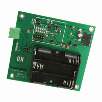
EVAL BOARD FOR NCP5030MTTXG
Manufacturer
ON Semiconductor
Datasheets
1.NCP5030MTTXG.pdf
(14 pages)
2.NCP5030MTTXGEVB.pdf
(1 pages)
3.NCP5030MTTXGEVB.pdf
(7 pages)
Specifications of NCP5030MTTXGEVB
Design Resources
NCP5030MTTXG EVB BOM NCP5030MTTXGEVB Gerber Files NCP5030MTTXG EVB Schematic
Current - Output / Channel
900mA
Outputs And Type
1, Non-Isolated
Voltage - Output
2.2 ~ 5.5 V
Features
Adjustable
Voltage - Input
2.7 ~ 5.5V
Utilized Ic / Part
NCP5030
Rohs Compliant
NO
Lead Free Status / RoHS Status
Lead free / RoHS Compliant
For Use With/related Products
NCP5030MTTXG
Other names
NCP5030MTTXGEVBOS
1. Visual inspection the board after solder, there should be no short, redundant solder ball.
2. Measure the resistance of each pin of NCP5030 to GND, there should be no short to GND
3. Short J104;
4. Short J103;
5. Short J106 2-3(power supply from J101);
6. Configure J102 in 2-3 position;
7. Short J105, open J111,J108;
8. Configure J109 in 100mA position (pin1-2 shorted);
9. Configure power supply output voltage to 3.7V.
10. Power off and connect power supply to J101;
11. Power on, check D101 is lighting;
12. Power off and Configure J109 in 200mA position (pin3-4 shorted);
13. Power on, check D101 is lighting;
14. Power off and Configure J109 in 400mA position (pin5-6 shorted);
15. Power on, check D101 is lighting;
16. Power off and Configure J109 in 400mA position (pin7-8 shorted);
17. Power on, check D101 is lighting;
18. Power off and configure J102 at 1-2 position;
19. Configure J109 in 100mA position (pin1-2 shorted);
20. Power on, check D101 is lighting;
21. Power off, open J105, short J111 (if D102 mounted);
22. Power on, check D102 is lighting (if D102 mounted);
23. Power off, open J105, J111, connect J108 to external LED or LED module (if there is);
24. Power on, check external LED or LED module is lighting (if there is);
25. Power off;
26. Configure board default and connect jumpers accordingly
12/19/2007
(except pin GND) or each other. Measure the forward and backward resistance of
D101/D102. Ensure solder is good.
• Place board in 900mA output current configuration:
• Place jumpers on J103/J104;
• Place a jumper on J105 and make sure J111 is open;
• Place a jumper on J106 2-3;
Test Procedure for the NCP5030MTTXG Evaluation Board
Place jumpers on J109 1-2/5-6/7-8;
Place a jumper on J102 2-3;
- 1 -
www.onsemi.com
Related parts for NCP5030MTTXGEVB
Image
Part Number
Description
Manufacturer
Datasheet
Request
R

Part Number:
Description:
ON Semiconductor [VOLTAGE REGULATOR]
Manufacturer:
ON Semiconductor
Datasheet:
Part Number:
Description:
357-036-542-201 CARDEDGE 36POS DL .156 BLK LOPRO
Manufacturer:
ON Semiconductor
Datasheet:
Part Number:
Description:
357-036-542-201 CARDEDGE 36POS DL .156 BLK LOPRO
Manufacturer:
ON Semiconductor
Datasheet:
Part Number:
Description:
357-036-542-201 CARDEDGE 36POS DL .156 BLK LOPRO
Manufacturer:
ON Semiconductor
Datasheet:
Part Number:
Description:
357-036-542-201 CARDEDGE 36POS DL .156 BLK LOPRO
Manufacturer:
ON Semiconductor
Datasheet:
Part Number:
Description:
357-036-542-201 CARDEDGE 36POS DL .156 BLK LOPRO
Manufacturer:
ON Semiconductor
Datasheet:
Part Number:
Description:
357-036-542-201 CARDEDGE 36POS DL .156 BLK LOPRO
Manufacturer:
ON Semiconductor
Datasheet:
Part Number:
Description:
357-036-542-201 CARDEDGE 36POS DL .156 BLK LOPRO
Manufacturer:
ON Semiconductor
Datasheet:
Part Number:
Description:
357-036-542-201 CARDEDGE 36POS DL .156 BLK LOPRO
Manufacturer:
ON Semiconductor
Datasheet:
Part Number:
Description:
357-036-542-201 CARDEDGE 36POS DL .156 BLK LOPRO
Manufacturer:
ON Semiconductor
Datasheet:
Part Number:
Description:
357-036-542-201 CARDEDGE 36POS DL .156 BLK LOPRO
Manufacturer:
ON Semiconductor
Datasheet:
Part Number:
Description:
Manufacturer:
ON Semiconductor
Datasheet:
Part Number:
Description:
Manufacturer:
ON Semiconductor
Datasheet:
Part Number:
Description:
Manufacturer:
ON Semiconductor
Datasheet: