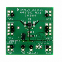
ADP1720-EVALZ Analog Devices Inc, ADP1720-EVALZ Datasheet

ADP1720-EVALZ
Specifications of ADP1720-EVALZ
Related parts for ADP1720-EVALZ
ADP1720-EVALZ Summary of contents
Page 1
... GENERAL DESCRIPTION The ADP1720 is a high voltage, micropower, low dropout linear regulator. Operating over a very wide input voltage range the ADP1720 can provide output current. With just 28 μA of quiescent supply current and a micropower shutdown mode, this device is ideal for applications that require low quiescent current ...
Page 2
... Change to Figure 1 ........................................................................... 1 Changes to Table 1 ............................................................................ 3 Changes to Ordering Guide .......................................................... 15 2/07—Revision 0: Initial Version Typical Performance Characteristics ..............................................7 Theory of Operation ...................................................................... 10 Adjustable Output Voltage (ADP1720 Adjustable) ............... 10 Applications Information .............................................................. 11 Capacitor Selection .................................................................... 11 Current Limit and Thermal Overload Protection ................. 11 Thermal Considerations ............................................................ 12 ...
Page 3
... Thermal Shutdown TS SD-HYS Hysteresis EN CHARACTERISTICS EN Input Logic High V IH Logic Low V IL Leakage Current V I-LEAKAGE ADJ INPUT BIAS CURRENT ADJ I-BIAS (ADP1720 ADJUSTABLE) = 25°C, unless otherwise noted. A Conditions T = –40°C to +125° μA OUT μ 0 (whichever is OUT IN OUT greater –40°C to +125°C ...
Page 4
... ADP1720 Parameter Symbol POWER SUPPLY REJECTION RATIO PSRR 1 Accuracy when OUT is connected directly to ADJ. When OUT voltage is set by external feedback resistors, absolute accuracy in adjust mode depends on the tolerances of resistors used. 2 Based on an end-point calculation using 1 mA and 50 mA loads. See Fi 3 Dropout voltage is defined as the input to output voltage differential when the input voltage is set to the nominal output voltage. This applies only for output voltages above 4 V ...
Page 5
... THERMAL RESISTANCE θ is specified for the worst-case conditions, that is, a device JA soldered in a circuit board for surface-mount packages. Table 3. Thermal Resistance Package Type 8-Lead MSOP ESD CAUTION Rev Page ADP1720 θ θ Unit JA JC 118 57 °C/W ...
Page 6
... Regulated Output Voltage. Bypass OUT to GND with a 1 μF or greater capacitor. Enable Input. Drive EN high to turn on the regulator; drive it low to turn off the regulator. For automatic startup, connect EN to IN. Ground. Ground. Ground. Ground. Rev Page ADJ GND 1 8 ADP1720 IN GND 2 7 ADJUSTABLE OUT 3 6 GND TOP VIEW (Not to Scale) ...
Page 7
... I (mA) LOAD Figure 9. Ground Current vs. Load Current 1400 I = 50mA LOAD I = 25mA LOAD I = 10mA 1200 LOAD 1000 800 600 400 200 (V) IN Figure 10. Ground Current vs. Input Voltage ADP1720 125 100 I = 1mA LOAD I = 100µA LOAD I = 10µA LOAD ...
Page 8
... ADP1720 300 250 200 150 100 (mA) LOAD Figure 11. Dropout Voltage vs. Load Current 5. 1mA LOAD 5.00 4.95 4. 50mA LOAD 4. 25mA LOAD 4. 10mA LOAD 4.75 4.70 4.65 4.60 4.9 5.0 5.1 5.2 V (V) IN Figure 12. Output Voltage vs. Input Voltage (in Dropout) 3.5 3.0 2.5 2.0 1 ...
Page 9
... OUT C = 1µ 1µF OUT LOAD STEP FROM 2.5mA TO 47.5mA V OUT 1 TIME (20µs/DIV) Figure 16. Load Transient Response 10mA 10M 1 2 Rev Page ADP1720 V STEP FROM OUT C = 1µ 1µF OUT I = 50mA LOAD V OUT TIME (100µs/DIV) Figure 17. Line Transient Response EN V ...
Page 10
... The adjustable output voltage can be set to between 1.225 V and 5 external voltage divider connected from OUT to ADJ. The ADP1720 uses the EN pin to enable and disable the OUT pin under normal operating conditions. When EN is high, OUT turns on; when EN is low, OUT turns off. For automatic startup, EN can be tied to IN ...
Page 11
... Consider the case where a hard short from OUT to GND occurs. At first, the ADP1720 current limits so that only conducted into the short. If self-heating of the junction is great enough to cause its temperature to rise above 150°C, thermal shutdown activates, turning off the output and reducing the output current to zero ...
Page 12
... ADP1720 THERMAL CONSIDERATIONS To guarantee reliable operation, the junction temperature of the ADP1720 must not exceed 125°C. To ensure the junction tem- perature stays below this maximum value, the user needs to be aware of the parameters that contribute to junction temperature changes. These parameters include ambient temperature, power dissipation in the power device, and thermal resistances between the junction and ambient air (θ ...
Page 13
... CURRENT – V (V) IN OUT 2 Figure 26. 100 mm of PCB Copper 50°C A 140 MAX T 120 100 1mA 5mA Figure 27 Rev Page ADP1720 (DO NOT OPERATE ABOVE THIS POINT) J 10mA 30mA 50mA 20mA 40mA (LOAD CURRENT – V (V) IN OUT 2 of PCB Copper 50° ...
Page 14
... PRINTED CIRCUIT BOARD LAYOUT CONSIDERATIONS Heat dissipation from the package can be improved by increasing the amount of copper attached to the pins of the ADP1720. How- ever, as can be seen from Table 5, a point of diminishing returns eventually is reached, beyond which an increase in the copper size does not yield significant heat dissipation benefits. ...
Page 15
... OUTLINE DIMENSIONS ORDERING GUIDE Model Temperature Range 1 ADP1720ARMZ-5-R7 –40°C to +125°C 1 ADP1720ARMZ-3.3-R7 –40°C to +125°C 1 ADP1720ARMZ-R7 –40°C to +125°C 1 ADP1720-5-EVALZ 1 ADP1720-3.3-EVALZ 1 ADP1720-EVALZ RoHS Compliant Part. 3.20 3.00 2.80 5. 3.20 4.90 3.00 4.65 2. PIN 1 0.65 BSC 0.95 0.85 1.10 MAX 0.75 8° ...
Page 16
... ADP1720 NOTES ©2007 Analog Devices, Inc. All rights reserved. Trademarks and registered trademarks are the property of their respective owners. D06111-0-7/07(A) Rev Page ...


