TMPSNSRD-TCPL1 Microchip Technology, TMPSNSRD-TCPL1 Datasheet - Page 13
TMPSNSRD-TCPL1
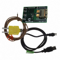
Manufacturer Part Number
TMPSNSRD-TCPL1
Description
BOARD RTD REFERENCE DESIGN
Manufacturer
Microchip Technology
Specifications of TMPSNSRD-TCPL1
Sensor Type
Temperature, Thermocouple
Embedded
No
Utilized Ic / Part
MCP3421, MCP9804
Processor To Be Evaluated
MCP9804, MCP3421
Interface Type
USB
Lead Free Status / RoHS Status
Lead free / RoHS Compliant
Voltage - Supply
-
Interface
-
Sensitivity
-
Sensing Range
-
Lead Free Status / Rohs Status
Lead free / RoHS Compliant


Inverting Amplifier with Programmable Gain Circuits
Programmable Amplifi er Gain Using a
Digital Potentiometer
Many sensors require their signal to be amplifi ed before
being converted to a digital representation. This signal gain
may be done with and operational amplifi er. Since all sensors
will have some variation in their operational characteristics,
it may be desireable to calibrate the gain of the operational
amplifi er to ensure an optimal output voltage range.
The fi gure below shows two inverting amplifi er with
programmable gain circuits. The generic circuit (a) where R
R
amplifi er, and the simplifi ed circuit (b) which removes
resistors R
R
The simplifi ed circuit reduces the cost and board area but
there are trade-offs (for the same resistance and resolution),
Using the R
to be limited and therefore each digital potentiometer step
is a fi ne adjust within that range. While in the simplifi ed
circuit, the range is not limited and therefore each digital
potentiometer step causes a larger variation in the gain.
The feedback capacitor (C
Programmable Gain Using Digital Potentiometers
Note 1: A general purpose op amp, such as the MCP6001.
V
2
AW
, and Pot
IN
and R
V
IN
BW
1
1
1
R
and R
can be used to tune the gain of the inverting
ratio to control the gain.
and R
1
A
W
Pot
2
2
A
and just uses the digital potentiometers
1
W
resistors allows the range of the gain
Simplified Circuit (b)
Pot
Generic Circuit (a)
B
1
F
) is used for circuit stability.
B
–
+
Op Amp
+
–
Op Amp
(1)
C
F
R
2
(1)
C
F
V
OUT
V
OUT
1
,
Equation 1-1 shows how to calcultate the gain for the
simplifi ed circuit (Figure 1-1b). The gain is the ratio of the
digital potentiometers wiper position on the R
ladder. As the wiper moves away from the midscale value,
the gain will either become greater then one (as wiper moves
towards Terminal A), or less then one (as wiper moves
towards Terminal B).
The device’s wiper resistance (R
calculations. This is due to it being in series with the op amp
input resistance and the op amp input impedence is very
large.
Circuit Gain Equation
R
R
BW
AW
= # of Resistors – Wiper Code x R
=
# of Resistors
R
# of Resistors
AB
V
OUT
= – R
x Wiper Code
R
BW
AW
W
Signal Chain Design Guide
) is ignored for fi rst order
x V
IN
AB
AB
resistor
13
Related parts for TMPSNSRD-TCPL1
Image
Part Number
Description
Manufacturer
Datasheet
Request
R

Part Number:
Description:
BOARD RTD REFERENCE DESIGN
Manufacturer:
Microchip Technology
Datasheet:

Part Number:
Description:
BOARD EVAL PT100 RTD TEMP SENSOR
Manufacturer:
Microchip Technology
Datasheet:

Part Number:
Description:
Manufacturer:
Microchip Technology Inc.
Datasheet:
Part Number:
Description:
Manufacturer:
Microchip Technology Inc.
Datasheet:
Part Number:
Description:
Manufacturer:
Microchip Technology Inc.
Datasheet:
Part Number:
Description:
Manufacturer:
Microchip Technology Inc.
Datasheet:
Part Number:
Description:
Manufacturer:
Microchip Technology Inc.
Datasheet:
Part Number:
Description:
Manufacturer:
Microchip Technology Inc.
Datasheet:
Part Number:
Description:
Manufacturer:
Microchip Technology Inc.
Datasheet:
Part Number:
Description:
Manufacturer:
Microchip Technology Inc.
Datasheet: