E1106 Atmel, E1106 Datasheet - Page 14
E1106
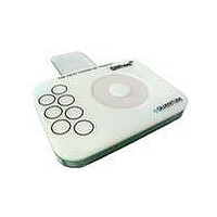
Manufacturer Part Number
E1106
Description
BOARD EVALUATION FOR QT1106-ISG
Manufacturer
Atmel
Specifications of E1106
Sensor Type
*
Sensing Range
*
Interface
*
Sensitivity
*
Voltage - Supply
*
Embedded
*
Utilized Ic / Part
*
Interface Type
USB
Lead Free Status / RoHS Status
Lead free / RoHS Compliant
For Use With/related Products
QT1106
Other names
E1106AT


5 Reset
5.1 Introduction
When starting from power-up or /RST reset there are a few
additional factors to be aware of. In most applications the
host will not need to take special action.
During hardware reset all outputs are disabled. To define the
levels of the CHANGE and DRDY during reset these signals
should pulled down by resistors to 0V. Otherwise, they may
drift high causing the host to detect a false logic 1.
When the initial reset phase ends, CHANGE and DRDY
outputs are enabled. DRDY will drive low and CHANGE will
drive high.
5.2 Delay to SPI Functionality
The QT1106 SPI interface is not operational while the device
is being reset. However, SPI is made operational early in the
start-up procedure.
After any reset (either via the /RST pin or via power-up), SPI
typically becomes operational within 100ms of /RST going
high or power-up. This is indicated to the host by DRDY
being pulsed high for at least 450µs, as occurs between
groups of acquire bursts when in Free Run mode. The
maximum delay is:
5.3 Reset Delay to Touch Detection
After power up or reset, the QT1106 calibrates all electrodes.
During this time, touch detection cannot be reported. Four
dummy bursts are performed in 80ms after exiting from the
reset start-up delay. Calibration completes after 14 burst
cycles, which normally requires an additional 280ms.
In total, 460ms are required from reset or power-up for the
device to be fully functional.
Disabled Keys: Keys with missing Cs capacitors, or that
otherwise have an out-of-range signal during calibration, are
considered to be unused or faulty and are disabled. Disabled
keys are re-examined for operation after each reset or
recalibration event.
5.4 Mode Setting After Reset
After a reset the device will enter Free Run mode, with AKS
disabled.
6 Design Notes
6.1 Oscillator Frequency
The oscillator uses an external network connected to the
OSC and SPREAD pins as shown in Figure 2.1. The charts
in this figure show the recommended values to use
depending on nominal operating voltage and
spread-spectrum mode.
If spread-spectrum mode is not used, only resistor R
be used, the Css capacitor eliminated, and the SPREAD pin
pulled to Vss with a 100k resistor.
An out-of-specification oscillator can induce timing problems
such as large variations in response times as well as on the
SPI port.
Lq
Vdd >= 4.5V: 150ms
Vdd < 4.5V:
200ms
B1
should
14
6.2 Spread-spectrum Circuit
The QT1106 offers the ability to spectrally spread its
frequency of operation to heavily reduce susceptibility to
external noise sources and to limit RF emissions. The
SPREAD pin is used to modulate an external passive RC
network that modulates the OSC pin. OSC is the main
oscillator current input. The circuit and recommended values
are shown in Figure 2.1.
The resistors Rb1 and Rb2 should be changed, depending
on Vdd. As shown in Figure 2.1, three sets of values are
recommended for these resistors, depending on Vdd. The
power curves in Section 7.6 also show the effect of these
resistors.
The spread-spectrum circuit can be eliminated if it is not
desired; see Section 6.1. Non spread-spectrum mode
consumes less current in the low power modes.
The spread-spectrum RC network should be adjusted to suit
the acquire burst lengths. The sawtooth waveform observed
on SPREAD should reach a crest height as follows:
The Css capacitor connected to SPREAD (see Figure 2.1)
should be adjusted so that the waveform approximates the
above amplitude, ±10 percent, during normal operation in the
target circuit. If this is done, the circuit will give a spectral
modulation of 12 to 15 percent.
In cases where the three acquire bursts 1, 2, 3 are of
different lengths, the Css capacitor should be adjusted for the
longest acquire burst.
6.3 Cs Sample Capacitors - Sensitivity
The Cs sample capacitors accumulate the charge from the
key electrodes and determine sensitivity. Higher values of Cs
make the corresponding sensing channel more sensitive. The
values of Cs can differ for each channel, permitting
differences in sensitivity from key to key or to balance
unequal sensitivities.
Unequal sensitivities can occur due to key size and
placement differences and stray wiring capacitances. More
stray capacitance on a sense trace will desensitize the
corresponding key; increasing the Cs for that key will
compensate for the loss of sensitivity.
The Cs capacitors can be virtually any plastic film or low to
medium-K ceramic capacitor. The ‘normal’ Cs range is 1nF to
100nF for the keys and 4.7nF to 220nF for the wheel/slider,
depending on the sensitivity required; the larger values of Cs
require better quality to ensure reliable sensing. Acceptable
capacitor types for most uses include PPS film,
polypropylene film, and NP0 and X7R ceramics. Lower grade
ceramics than X7R are not advised; the X5R grade should be
avoided because it is less stable than X7R.
Vdd >= 3.6V:
Vdd < 3.6V:
17 percent of Vdd
20 percent of Vdd
QT1106_8IR0.07_0907
Related parts for E1106
Image
Part Number
Description
Manufacturer
Datasheet
Request
R

Part Number:
Description:
BOARD EVAL FOR QT110 TOUCH SENSR
Manufacturer:
Atmel
Datasheet:

Part Number:
Description:
DEV KIT FOR AVR/AVR32
Manufacturer:
Atmel
Datasheet:

Part Number:
Description:
INTERVAL AND WIPE/WASH WIPER CONTROL IC WITH DELAY
Manufacturer:
ATMEL Corporation
Datasheet:
Part Number:
Description:
Low-Voltage Voice-Switched IC for Hands-Free Operation
Manufacturer:
ATMEL Corporation
Datasheet:
Part Number:
Description:
MONOLITHIC INTEGRATED FEATUREPHONE CIRCUIT
Manufacturer:
ATMEL Corporation
Datasheet:
Part Number:
Description:
AM-FM Receiver IC U4255BM-M
Manufacturer:
ATMEL Corporation
Datasheet:
Part Number:
Description:
Monolithic Integrated Feature Phone Circuit
Manufacturer:
ATMEL Corporation
Datasheet:
Part Number:
Description:
Multistandard Video-IF and Quasi Parallel Sound Processing
Manufacturer:
ATMEL Corporation
Datasheet:
Part Number:
Description:
High-performance EE PLD
Manufacturer:
ATMEL Corporation
Datasheet:
Part Number:
Description:
8-bit Flash Microcontroller
Manufacturer:
ATMEL Corporation
Datasheet:
Part Number:
Description:
2-Wire Serial EEPROM
Manufacturer:
ATMEL Corporation
Datasheet: