C8051F930DK Silicon Laboratories Inc, C8051F930DK Datasheet - Page 19
C8051F930DK
Manufacturer Part Number
C8051F930DK
Description
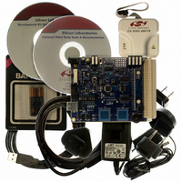
KIT DEV C8051F920,F921,F930,F931
Manufacturer
Silicon Laboratories Inc
Type
MCUr
Specifications of C8051F930DK
Contents
Target Board, Power Adapter, USB Debug Adapter, Cables, Batteries, and Software
Processor To Be Evaluated
C8051F930
Processor Series
C8051F9xx
Data Bus Width
8 bit
Interface Type
I2C, UART, SPI
Maximum Operating Temperature
+ 85 C
Minimum Operating Temperature
- 40 C
Operating Supply Voltage
0.9 V to 3.6 V
Lead Free Status / RoHS Status
Lead free / RoHS Compliant
For Use With/related Products
C8051F920, F921, F930, F931
Lead Free Status / Rohs Status
Lead free / RoHS Compliant
Other names
336-1473
Available stocks
Company
Part Number
Manufacturer
Quantity
Price
Company:

Part Number:
C8051F930DK
Manufacturer:
Silicon Labs
Quantity:
135


7.7. Target Board DEBUG Interface (J9)
The DEBUG connector J9 provides access to the DEBUG (C2) pins of the C8051F930. It is used to connect the
Serial Adapter or the USB Debug Adapter to the target board for in-circuit debugging and Flash programming.
Table 3 shows the DEBUG pin definitions.
7.8. Serial Interface (J12)
A USB-to-UART bridge circuit (U3) and USB connector (P3) are provided on the target board to facilitate serial
connections to UART0 of the C8051F930. The Silicon Labs CP2103 (U3) USB-to-UART bridge provides data
connectivity between the C8051F930 and the PC via a USB port. The VIO power supply and TX, RX, RTS and
CTS signals of UART0 may be connected to the CP2103 by installing shorting blocks on header J12. The shorting
block positions for connecting each of these signals to the CP2103 are listed in Table 4. To use this interface, the
USB-to-UART device drivers should be installed as described in Section 3.2. "CP210x USB to UART VCP Driver
Installation‚" on page 2.
7.9. Analog I/O (H1)
Several of the C8051F930 target device’s port pins are connected to the H1 terminal block. Refer to Table 5 for the
H1 terminal block connections.
Table 4. Serial Interface Header (J12) Description
Table 3. DEBUG Connector Pin Descriptions
Table 5. H1 Terminal Block Pin Descriptions
Header Pins UART0 Pin Description
2, 3, 9
Pin #
Pin #
J12[9–10]
J12[7–8]
J12[5–6]
J12[3–4]
J12[1–2]
10
1
4
5
6
7
8
1
2
3
4
P0.0/V
USB Power (+5 VDC from J9)
CP2103_VIO (VDD/DC+)
+3 VD (+3.3 VDC)
REF
Rev. 0.5
Not Connected
GND (Ground)
P0.6/CNVSTR
GND (Ground)
Description
Description
RST (Reset)
P0.7/IREF0
RST/C2CK
P2.7/C2D
TX_MCU (P0.5)
RX_MCU (P0.4)
(Voltage Reference)
P2.7
RTS (P0.6)
CTS (P0.7)
C8051F930-DK
19
Related parts for C8051F930DK
Image
Part Number
Description
Manufacturer
Datasheet
Request
R

Part Number:
Description:
SMD/C°/SINGLE-ENDED OUTPUT SILICON OSCILLATOR
Manufacturer:
Silicon Laboratories Inc
Part Number:
Description:
Manufacturer:
Silicon Laboratories Inc
Datasheet:
Part Number:
Description:
N/A N/A/SI4010 AES KEYFOB DEMO WITH LCD RX
Manufacturer:
Silicon Laboratories Inc
Datasheet:
Part Number:
Description:
N/A N/A/SI4010 SIMPLIFIED KEY FOB DEMO WITH LED RX
Manufacturer:
Silicon Laboratories Inc
Datasheet:
Part Number:
Description:
N/A/-40 TO 85 OC/EZLINK MODULE; F930/4432 HIGH BAND (REV E/B1)
Manufacturer:
Silicon Laboratories Inc
Part Number:
Description:
EZLink Module; F930/4432 Low Band (rev e/B1)
Manufacturer:
Silicon Laboratories Inc
Part Number:
Description:
I°/4460 10 DBM RADIO TEST CARD 434 MHZ
Manufacturer:
Silicon Laboratories Inc
Part Number:
Description:
I°/4461 14 DBM RADIO TEST CARD 868 MHZ
Manufacturer:
Silicon Laboratories Inc
Part Number:
Description:
I°/4463 20 DBM RFSWITCH RADIO TEST CARD 460 MHZ
Manufacturer:
Silicon Laboratories Inc
Part Number:
Description:
I°/4463 20 DBM RADIO TEST CARD 868 MHZ
Manufacturer:
Silicon Laboratories Inc
Part Number:
Description:
I°/4463 27 DBM RADIO TEST CARD 868 MHZ
Manufacturer:
Silicon Laboratories Inc
Part Number:
Description:
I°/4463 SKYWORKS 30 DBM RADIO TEST CARD 915 MHZ
Manufacturer:
Silicon Laboratories Inc
Part Number:
Description:
N/A N/A/-40 TO 85 OC/4463 RFMD 30 DBM RADIO TEST CARD 915 MHZ
Manufacturer:
Silicon Laboratories Inc
Part Number:
Description:
I°/4463 20 DBM RADIO TEST CARD 169 MHZ
Manufacturer:
Silicon Laboratories Inc