DV164039 Microchip Technology, DV164039 Datasheet - Page 36
DV164039
Manufacturer Part Number
DV164039
Description
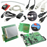
KIT DEV PIC24FJ256DA210
Manufacturer
Microchip Technology
Series
dsPIC™r
Type
MCUr
Specifications of DV164039
Contents
Dev Board, Display Board, 3 Bare Boards, MPLAB ICD-3, Cables, Power Supply
Processor To Be Evaluated
PIC24FJ256DA210
Data Bus Width
16 bit
Interface Type
RS-232, USB, Ethernet, SPI, UART
Operating Supply Voltage
9 V to 15 V
Silicon Manufacturer
Microchip
Core Architecture
PIC
Core Sub-architecture
PIC24
Silicon Core Number
PIC24F
Silicon Family Name
PIC24FJxxDAxxx
Lead Free Status / RoHS Status
Lead free / RoHS Compliant
For Use With/related Products
PIC24FJ256DA210
Lead Free Status / Rohs Status
Lead free / RoHS Compliant
Available stocks
Company
Part Number
Manufacturer
Quantity
Price
Company:

Part Number:
DV164039
Manufacturer:
MICROCHIP
Quantity:
12 000
Part Number:
DV164039
Manufacturer:
MICROCHIP/微芯
Quantity:
20 000


PIC24FJ256DA210 Development Board User’s Guide
DS51911A-page 36
FIGURE 4-3:
TABLE 4-3:
4.4.1.1
The development board comes with three general purpose switches, S1, S2 and S3,
for user inputs. The push button switches are normally pulled up to V
unpressed, and pulled to ground when pressed.
To enable the switches:
1. To enable switch S1 (Figure 4-3, callout 1):
2. To enable switch S2 (Figure 4-3, callout 2):
3. To enable switch S3 (Figure 4-3, callout 3):
JP13
JP14
JP15
Jumper
a) Set jumper JP13 to bridge RG8-S1 (default).
b) Populate resistor R25 with a
c) If installed, remove resistors R26 and R27 (not populated by default)
a) Set jumper JP14 to bridge RE9-S2 (default)
b) Populate resistor R31 with a
c) If installed, remove resistor R32 (not populated by default)
a) Set jumper JP15 to bridge RB5-S3
b) Populate resistor R41 with a
c) If installed, remove resistor R45 (not populated by default)
USER-DEFINED PUSH BUTTONS (S1, S2 AND S3)
RG8 is push button S1 input (default)
RG8 is CTMU Pad 1 input and LED D1 output
RE9 is push button S2 input (default)
RE9 is CTMU Pad 2 input and LED D2 output
RB5 is push button S3 input
RB5 is CTMU Pad 3 input and LED D3 output
RB5 is potentiometer (R3) input (default)
JUMPER SETTINGS FOR RB5, RE9 AND RG8 INPUTS
CONFIGURATION OF USER-DEFINED FEATURES
Configuration
0
0
0
resistor (default)
resistor (default)
resistor (default)
M
1
2
2010 Microchip Technology Inc.
3
DD
RG8–S1
PAD1–RG8
RE9–S2
PAD2–RE9
RB5–S3
PAD3–RB5
RB5–POT
when
Jumper
Setting
Related parts for DV164039
Image
Part Number
Description
Manufacturer
Datasheet
Request
R

Part Number:
Description:
Manufacturer:
Microchip Technology Inc.
Datasheet:
Part Number:
Description:
Manufacturer:
Microchip Technology Inc.
Datasheet:
Part Number:
Description:
Manufacturer:
Microchip Technology Inc.
Datasheet:
Part Number:
Description:
Manufacturer:
Microchip Technology Inc.
Datasheet:
Part Number:
Description:
Manufacturer:
Microchip Technology Inc.
Datasheet:
Part Number:
Description:
Manufacturer:
Microchip Technology Inc.
Datasheet:
Part Number:
Description:
Manufacturer:
Microchip Technology Inc.
Datasheet:
Part Number:
Description:
Manufacturer:
Microchip Technology Inc.
Datasheet: