PK-ST7FLITE2 SofTec Microsystems SRL, PK-ST7FLITE2 Datasheet
PK-ST7FLITE2
Manufacturer Part Number
PK-ST7FLITE2
Description
KIT STARTER USB FOR ST7FLITE2
Manufacturer
SofTec Microsystems SRL
Type
MCUr
Specifications of PK-ST7FLITE2
Contents
Board, Cable, Software, Datasheets and User Manual
Silicon Manufacturer
ST Micro
Features
Built-in Debug, In-Circuit Communication Serial Interface
Kit Contents
Board, Cable, CD
Silicon Family Name
ST7
Silicon Core Number
ST7FLITE2
Core Architecture
ARM
Core Sub-architecture
ARM7TDMI
Rohs Compliant
No
Lead Free Status / RoHS Status
Contains lead / RoHS non-compliant
For Use With/related Products
STMicro ST72FLITE2 (USB)
Lead Free Status / RoHS Status
Contains lead / RoHS non-compliant, Contains lead / RoHS non-compliant
Other names
520-1030


CLKIN
RESET
OSC1
OSC2
VDD
VSS
CLKIN/AIN4/PB4
MISO/AIN2/PB2
MOSI/AIN3/PB3
0000h
007Fh
0080h
0200h
1000h
1100h
DFFFh
01FFh
0FFFh
10FFh
E000h
FFFFh
SCK/AIN1/PB1
SS/AIN0/PB0
AIN5/PB5
AIN6/PB6
ST7FLITE2
Easy Reference
RESET
PROGRAM MEMORY
VDD
INTERNAL CLOCK
VSS
DEBUG MODULE
POWER SUPPLY
DATA EEPROM
GENERATOR
(384 BYTES)
(256 BYTES)
WATCHDOG
(8K BYTES)
CONTROL
8-BIT ALU
RAM
LVD
(HS): 20 mA High-Sink Capability
eix: Associated External Interrupt Vector
1
2
3
4
5
6
7
8
9
10
FLASH MEMORY
ei3
ei2
DATA EEPROM
HW Registers
(8192 BYTES)
(384 Bytes)
(256 Bytes)
RESERVED
RESERVED
RAM
ei0
ei1
20
19
18
17
16
15
14
13
12
11
Memory Map
Block
Diagram
OSC1/CLKIN
OSC2
PA0 (HS)/LTIC
PA1 (HS)/ATIC
PA2 (HS)/ATPWM0
PA3 (HS)/ATPWM1
PA4 (HS)/ATPWM2
PA5 (HS)/ATPWM3/ICCDATA
PA6/MCO/ICCCLK/BREAK
PA7 (HS)
8-BIT LITE TIMER 2
RELOAD TIMER 2
ADC + OP AMP
12-BIT AUTO-
PA7
PA6/MCO/ICCCLK/BREAK
PA5/ATPWM3/ICCDATA
PA4/ATPWM2
PA3/ATPWM1
PA2/ATPWM0
PA1/ATIC
PA0/LTIC
PB6/AIN6
PB5/AIN5
PB4/AIN4/CLKIN
PB3/AIN3/MOSI
PB2/AIN2/MISO
PB1/AIN1/SCK
PB0/AIN0/SS
SPI
FFDEh
FFDFh
0080h
00FFh
0100h
01FFh
1000h
1001h
FFE0h
FFFFh
20-Pin SO
Package
SHORT ADDRESSING RAM (ZERO PAGE)
INTERRUPT AND RESET VECTORS
16-BIT ADDRESSING RAM
STACK (UP TO 128 BYTES)
VSS
RCCR0
RCCR1
RCCR0
RCCR1
POWER
+5 V
VSS
FUSE
USB D+
USB D-
+5 V
VSS
USB TO ICC
INTERFACE
RESET VALUE = RESET VECTOR @ FFFEh-FFFFh
RESET VALUE = STACK HIGHER ADDRESS
15
15
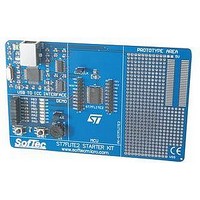
1. “USB to ICC Interface” Section
Contains the circuitry needed to
electrically and logically translate
ICC-like commands sent by the
host PC through the USB cable to
the ICC interface of the
microcontroller. The PK-ST7FLITE2
board is powered by the USB bus.
PCH
Microcontroller Development Tools
1
8
SP
CPU Registers
RESET VALUE = XXh
RESET VALUE = XXh
RESET VALUE = XXh
RESET VALUE = 111x1xxxb
1 1
7
7
7
7
2. “Demo” Section
Features a RESET push-button,
one user push-button, a
potentiometer and eight user
LEDs.
www.softecmicro.com
1
RESET
PCL
OSC_CLK
H
ICCDATA
ICCCLK
RESET
A
X
Y
ENABLE
I N Z C
2
+5 V
VSS
0
0
0
0
0
PB3
3. “MCU” Section
Contains a soldered, 20-pin
ST7FLITE2 device (in SOIC
package) with connectors to
access the I/O pins of the
microcontroller for expansion
prototyping.
ACCUMULATOR (A)
INDEX REGISTER (X)
INDEX REGISTER (Y)
PROGRAM COUNTER (PC)
CONDITION CODE REGISTER (CC)
STACK POINTER (SP)
PB2
3
PB1
MCU
PB0
PA3
4. “Prototype” Section
You can wire your own circuit
here. The prototype section
features both a standard, thru-
hole area (for mounting
traditional components) and a
SMD area (for soldering SMD
components in SOIC package).
VSS
4
PA2
PA1
PA0
OSC1
OSC2
PA7
OSC_CLK
PA [0..7]
PB [0..6]
RESET
ENABLE
Mnemonic
ADC d, s
ADD d, s
AND d, s
BCP s, d
BRES d, b
BSET d, b
BTJF d, b, rel
BTJT d, b, rel
CALL d
CALLR d
CLR d
CP d, s
CPL d
DEC d
HALT
INC d
IRET
JP d
JRA d
JRT d
JRF d
JRIH d
JRIL d
JRH d
JRNH d
JRM d
JRNM d
JRMI d
JRPL d
JREQ d
JRNE d
JRC d
JRNC d
JRULT d
JRUGE d
JRUGT d
JRULE d
LD d, s
MUL d, s
NEG d
NOP
OR d, s
POP d
PUSH d
RCF
RET
RIM
RLC d
RRC d
RSP
SBC d, s
SCF
SIM
SLA d
SLL d
SRA d
SRL d
SUB d, s
SWAP d
TNZ d
TRAP
WFI
XOR d, s
+5 V
VSS
Description
Add with carry, s to d
Add s to d
Logical AND (d with s)
Bit compare
Bit reset
Bit set
Jump if bit is false (0)
Jump if bit is true (1)
Call subroutine
Call subroutine relative
Clear d
Arithmetic compare
Logical 1-complement of d
Decrement d
Halt
Increment d
Interrupt routine return
Absolute jump
Jump relative always
Jump relative always
Never jump
Jump Relative if Port INT pin = 1
Jump Relative if Port INT pin = 0
Jump Relative if H = 1
Jump Relative if H = 0
Jump Relative if I = 1
Jump Relative if I = 0
Jump Relative if N = 1
Jump Relative if N = 0
Jump Relative if Z = 1
Jump Relative if Z = 0
Jump Relative if C = 1
Jump Relative if C = 0
Jump Relative if C = 1
Jump Relative if C = 0
Jump Relative if (C + Z) = 0
Jump Relative if (C + Z) = 1
Load s in d
Multiply d by s
Negate d (logical 2-complement)
No operation
Logical OR (d with s)
Pop from the Stack
Push onto the Stack
Reset carry flag
Subroutine return
Reset interrupt mask
Rotate left through carry
Rotate right through carry
Reset Stack pointer
Subtract s from d with carry
Set carry flag
Set interrupt mask
Shift left arithmetic (equal to SLL d)
Shift left logical
Shift right arithmetic
Shift right logical
Subtract s from d
Swap nibbles
Test for negative and zero
Software interrupt
Wait for interrupt
Logical exclusive OR (d with s)
+5 V
SIGNAL PINS
PB5
Instruction Set
Operation
d
d
d
{N, Z}
d
d
PC
PC
PUSH (PC); PC
PUSH (PC); PC
d
{N, Z, C}
d
d
I
d
POP CC, A, X, PC
PC
PC
PC
-
PC
PC
PC
PC
PC
PC
PC
PC
PC
PC
PC
PC
PC
PC
PC
PC
d
d:s
d
-
d
d
(SP- -)
C
POP PC
I
SP
d
C
I
d
d (7:4)
{N, Z}
PC
I
d
C
C
C
C
0
7
0
0
7
7
1
7
7
7
0
d + s + C
d + s
d AND s
d AND (NOT (2
d OR (2
0
d XOR FFh, or FFh - d
d - 1
d + 1
s
(d XOR FFh) + 1
d OR s
(++SP)
0
d - s - C
1
d - s
d XOR s
PC + rel IF (d AND (2
PC + rel IF (d AND (2
d
PC + d
PC + d
PC + d IF interrupt line high
PC + d IF interrupt line low
PC + d IF H = 1
PC + d IF H = 0
PC + d IF I = 1
PC + d IF I = 0
PC + d IF N = 1
PC + d IF N = 0
PC + d IF Z = 1
PC + d IF Z = 0
PC + d IF C = 1
PC + d IF C = 0
PC + d IF C = 1
PC + d IF C = 0
PC + d IF (C OR Z) = 0
PC + d IF (C OR Z) = 1
d * s
reset value
PC + 1; PUSH PC, X, A, CC; PC
s AND d
TEST (d)
d
d (3:0)
TEST (d - s)
b
)
0
Block Diagram
d
PC + d
0
0
0
0
0
C
b
))
0
0
C
PK-ST7FLITE2
+5 V
VSS
b
b
)) = 0
)) 0
trap vector
PROTOTYPE AREA
Dest.
A
A
A
A
mem
mem
mem
mem
mem
mem
reg, mem
reg
reg, mem
reg, mem
-
reg, mem
-
mem
mem
mem
mem
mem
mem
mem
mem
mem
mem
mem
mem
mem
mem
mem
mem
mem
mem
mem
mem
reg, mem
reg
reg, mem
-
A
reg
-
-
-
-
reg, mem
reg, mem
-
A
-
-
reg, mem
reg, mem
reg, mem
reg, mem
A
reg, mem
reg, mem
-
-
A
Source
mem
mem
mem
mem
-
-
-
-
-
-
-
mem
-
-
-
-
-
-
-
-
-
-
-
-
-
-
-
-
-
-
-
-
-
-
-
-
-
reg, mem
reg
-
-
mem
-
reg
-
-
-
-
-
-
mem
-
-
-
-
-
-
mem
-
-
-
-
mem
Flags
H, N, Z, C
H, N, Z, C
N, Z
N, Z
-
-
C
C
-
-
N = 0, Z = 1
N, Z, C
N, Z, C = 1
N, Z
I = 0
N, Z
H, I, N, Z, C
-
-
-
-
-
-
-
-
-
-
-
-
-
-
-
-
-
-
-
-
N, Z
H = 0, C = 0
N, Z, C
-
N, Z
H, I, N, Z, C
-
C = 0
-
I = 0
N, Z, C
N, Z, C
-
N, Z, C
C = 1
I = 1
N, Z, C
N, Z, C
N, Z, C
N = 0, Z, C
N, Z, C
N, Z
N, Z
I = 1
I = 0
N, Z
Related parts for PK-ST7FLITE2
Image
Part Number
Description
Manufacturer
Datasheet
Request
R


Part Number:
Description:
PROG HEAD FOR MP8011A 44-PLCC
Manufacturer:
SofTec Microsystems SRL

Part Number:
Description:
KIT STARTER USB FOR MC9S08GB60
Manufacturer:
SofTec Microsystems SRL
Datasheet:

Part Number:
Description:
KIT STARTER USB FOR MC68HC908QY4
Manufacturer:
SofTec Microsystems SRL
Datasheet:

Part Number:
Description:
KIT DESIGN FOR ST7
Manufacturer:
SofTec Microsystems SRL
Datasheet:
Part Number:
Description:
KIT DESIGN USB FOR HCO8
Manufacturer:
SofTec Microsystems SRL
Datasheet:
Part Number:
Description:
KIT DESIGN USB FOR HCO8
Manufacturer:
SofTec Microsystems SRL
Datasheet:

Part Number:
Description:
KIT DESIGN USB FOR HCO8
Manufacturer:
SofTec Microsystems SRL
Datasheet:
Part Number:
Description:
KIT DESIGN USB FOR HCO8
Manufacturer:
SofTec Microsystems SRL
Datasheet:
Part Number:
Description:
KIT DESIGN USB FOR HCS12
Manufacturer:
SofTec Microsystems SRL
Datasheet:
Part Number:
Description:
KIT DESIGN USB FOR HCS12
Manufacturer:
SofTec Microsystems SRL
Datasheet:
Part Number:
Description:
KIT DESIGN USB FOR HCS12
Manufacturer:
SofTec Microsystems SRL
Datasheet:
Part Number:
Description:
KIT DESIGN USB FOR HCO8
Manufacturer:
SofTec Microsystems SRL
Datasheet:
Part Number:
Description:
KIT DESIGN USB FOR HCO8
Manufacturer:
SofTec Microsystems SRL
Datasheet:
Part Number:
Description:
KIT DESIGN USB FOR HCO8
Manufacturer:
SofTec Microsystems SRL
Datasheet:
PK-ST7FLITE2 Summary of contents
Page 1
... ICC-like commands sent by the potentiometer and eight user package) with connectors to host PC through the USB cable to LEDs. access the I/O pins of the the ICC interface of the microcontroller for expansion microcontroller. The PK-ST7FLITE2 prototyping. board is powered by the USB bus MCU USB TO ICC ...
Page 2
... Copyright © 2004 SofTec Microsystems®. DC00737 3 Connect the Board to the PC Connect PK-ST7FLITE2 to a free USB port on your PC. The green “POWER” LED on the instrument will turn on. 5 Run STVD7 and Open the Example Start STMicroelectronics Visual Debug for ST7 (STVD7) by selecting Start > ...