AD8330-EVAL Analog Devices Inc, AD8330-EVAL Datasheet - Page 17
AD8330-EVAL
Manufacturer Part Number
AD8330-EVAL
Description
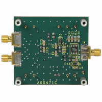
BOARD EVAL FOR AD8330
Manufacturer
Analog Devices Inc
Specifications of AD8330-EVAL
Rohs Status
RoHS non-compliant


Another gain related feature allows both gain control ranges
to be accurately raised by 200 mV. To enable this offset, open
circuit CMGN (Pin 6, LFCSP; Pin 8, LQFP) and add a 0.1 μF
capacitor to ground. In use, the nominal range for V
from 0.2 V to 1.7 V and V
specifications apply for any supply voltage. This allows the use
of DACs whose output range does not include ground as sources
for the gain control function(s).
Note that the 200 mV that appears on this pin affects the
response to an externally applied V
unconnected, the internally set default value of 0.5 V still applies.
Furthermore, Pin CMGN can, if desired, be driven by a user-
supplied voltage to reposition the baseline for V
externally applied V
all cases, the gain scaling, its law conformance, and temperature
stability are unaffected.
Two Classes of Variable Gain Amplifiers
Note that there are two broad classes of VGAs. The first type is
designed to cope with a very wide range of input amplitudes
and, by virtue of its gain control function, compress this range
down to an essentially constant output. This is the function
needed in an AGC system. Such a VGA is called an IVGA,
referring to a structure optimized to address a wide range of
input amplitudes. By contrast, an OVGA is optimized to deliver
a wide range of output values while operating with an essentially
constant input amplitude. This function might be needed, for
example, in providing a variable drive to a power amplifier.
It is apparent from the foregoing sections that the AD8330 is
both an IVGA and an OVGA in one package. This is an unusual
and possibly confusing degree of versatility for a VGA; therefore,
these two distinct control functions are described at separate
points throughout this data sheet to explain the operation and
applications of this product. It is, nevertheless, useful to briefly
describe the capabilities of these features when used together.
–0.05
–0.10
0.10
0.05
–0.5
–1.0
–1.5
–2.0
1.0
0.8
0.6
0.4
2.5
2.0
1.5
1.0
0.5
1.2
0.2
–400
0
0
0
–300
Figure 50. Using VMAG in Modulation Mode
MAG
–200
) to any other voltage up to 500 mV. In
MAG
–100
TIME (ns)
V
from 0.2 V to 5.2 V. These
V
V
MAG
OUT
IN
MAG
0
, but when Pin VMAG is
100
DBS
200
(or for an
DBS
300
extends
Rev. E | Page 17 of 32
Amplitude/Phase Response
The ac response of the AD8330 is remarkably consistent not
only over the full 50 dB of its basic gain range, but also with
changes of gain due to alteration of V
Figure 51. This is an overlay of two sets of results: first, with a
very low V
[20 × log10(500 mV/16 mV)]; second, with V
increases the gain by 20 dB = 20 × log10(5 V/0.5 V).
This 50 dB step change in gain produces two sets of gain curves,
having a total gain span of 100 dB. It is apparent that the ampli-
tude and phase response are essentially independent of the gain
over this wide range, an aspect of the AD8330 performance
potential unprecedented in any prior VGA.
It is unusual for an application to require such a wide range of
gains; and, as a practical matter, the peak output voltage for
V
nominal value of ±2 V, to only ±64 mV. As previously noted,
most applications of VGAs require that they operate in a mode
that is predominantly of either an IVGA or OVGA style, rather
than mixed modes.
With this limitation in mind, and simply to illustrate the unusual
possibilities afforded by the AD8330, note that, with appropriate
drive to V
120 dB, extending from −50 dB to +70 dB, as shown in Figure 52
for operation at 1 MHz and 100 MHz. In this case, V
V
varies from 1.2 mV to 5 V, with 30% (1.5/5) of V
to V
The gain varies in a linear-in-dB manner with V
the response from V
overall numerical gain as the product of these two functions is
In rare cases where such a wide gain range is of value, the
calibration is still accurate and the temperature is stable.
MAG
MAG
DBS
Figure 51. AC Performance over a 100 dB Gain Range Obtained by
GAIN
–100
–150
–200
–250
–300
–350
= 16 mV is reduced by the factor 16/500, compared to its
are driven from a common control voltage, V
–10
–30
–50
–50
, and 100% applied to V
90
70
50
30
10
100k
0
10k
DBS
MAG
=
and V
V
of 16 mV that reduces the overall gain by 30 dB
GAIN
100k
MAG
MAG
0 /
Using Two Values of V
1M
5 .
is linear-in-magnitude. Consequently, the
in tandem, the gain span is a remarkable
V
×
FREQUENCY (Hz)
0
3 .
1M
MAG
×
10
.
10M
V
0
GAIN
6 .
MAG
V
10M
MAG
, as demonstrated in
MAG
G = –20dB
DBS
GAIN
100M
G = +70dB
= 5 V that
100M 300M
GAIN
, although
AD8330
DBS
applied
, that
300M
and
(7)
Related parts for AD8330-EVAL
Image
Part Number
Description
Manufacturer
Datasheet
Request
R

Part Number:
Description:
BOARD EVAL FOR AD8330
Manufacturer:
Analog Devices Inc
Datasheet:

Part Number:
Description:
±1.7g Dual-Axis IMEMS Accelerometer Evaluation Board
Manufacturer:
Analog Devices Inc
Datasheet:

Part Number:
Description:
Inertial Sensor Evaluation System
Manufacturer:
Analog Devices Inc
Datasheet:
Part Number:
Description:
Manufacturer:
Analog Devices Inc
Datasheet:
Part Number:
Description:
Manufacturer:
Analog Devices Inc
Datasheet:
Part Number:
Description:
Manufacturer:
Analog Devices Inc
Datasheet:
Part Number:
Description:
Manufacturer:
Analog Devices Inc
Datasheet:
Part Number:
Description:
Manufacturer:
Analog Devices Inc
Datasheet:
Part Number:
Description:
Manufacturer:
Analog Devices Inc
Datasheet:
Part Number:
Description:
Manufacturer:
Analog Devices Inc
Datasheet:
Part Number:
Description:
Manufacturer:
Analog Devices Inc
Datasheet:
Part Number:
Description:
Manufacturer:
Analog Devices Inc
Datasheet:
Part Number:
Description:
Manufacturer:
Analog Devices Inc
Datasheet: