EVAL-AD7731EB Analog Devices Inc, EVAL-AD7731EB Datasheet - Page 31
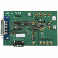
EVAL-AD7731EB
Manufacturer Part Number
EVAL-AD7731EB
Description
BOARD EVAL FOR AD7731
Manufacturer
Analog Devices Inc
Specifications of EVAL-AD7731EB
Number Of Adc's
1
Number Of Bits
24
Sampling Rate (per Second)
6.4k
Data Interface
Serial
Inputs Per Adc
3 Differential
Input Range
±1.28 V
Power (typ) @ Conditions
67.5mW @ 6.4kSPS
Voltage Supply Source
Analog and Digital
Operating Temperature
-40°C ~ 85°C
Utilized Ic / Part
AD7731
Lead Free Status / RoHS Status
Contains lead / RoHS non-compliant


The system full-scale calibration needs to be performed as one
part of a two part full calibration. However, once a full calibra-
tion has been performed, additional system full-scale calibra-
tions can be performed by themselves to adjust the part’s gain
calibration point only. When performing a two-step full calibra-
tion, care should be taken as to the sequence in which the two
steps are performed. A system full-scale calibration should not
be carried out unless the part contains valid zero-scale coeffi-
cients. Therefore, an internal zero-scale calibration or a system
zero-scale calibration must be performed before the system full-
scale calibration when a full two-step calibration operation is
being performed.
Span and Offset Limits
Whenever a system calibration mode is used, there are limits on
the amount of offset and span that can be accommodated. The
overriding requirement in determining the amount of offset and
gain that can be accommodated by the part is the requirement
that the positive full-scale calibration limit is 1.05 FS, where
FS is 20 mV through 1.28 V depending on the RN2, RN1, RN0
bits in the Mode Register. This allows the input range to go 5%
above the nominal range. The built-in headroom in the AD7731’s
analog modulator ensures that the part will still operate correctly
with a positive full-scale voltage that is 5% beyond the nominal.
The range of input span in both the unipolar and bipolar modes
has a minimum value of 0.8 FS and a maximum value of
2.1 FS. However, the span (which is the difference between
the bottom of the AD7731’s input range and the top of its input
range) has to take into account the limitation on the positive
full-scale voltage. The amount of offset which can be accommo-
dated depends on whether the unipolar or bipolar mode is being
used. Once again, the offset has to take into account the limita-
tion on the positive full-scale voltage. In unipolar mode, there is
considerable flexibility in handling negative (with respect to
AIN[–]) offsets. In both unipolar and bipolar modes, the range
of positive offsets that can be handled by the part depends on
the selected span. Therefore, in determining the limits for sys-
tem zero-scale and full-scale calibrations, the user has to ensure
that the offset range plus the span range does not exceed
1.05 FS. This is best illustrated by looking at a few examples.
If the part is used in unipolar mode with a required span of
0.8 FS, the offset range the system calibration can handle is
from –1.05 FS to +0.25 FS. If the part is used in unipolar
mode with a required span of FS, the offset range the system
calibration can handle is from –1.05 FS to +0.05 FS. Simi-
larly, if the part is used in unipolar mode and required to remove
an offset of 0.2 FS, the span range the system calibration can
handle is 0.85 FS.
If the part is used in bipolar mode with a required span of
from –0.65 FS to +0.65 FS. If the part is used in bipolar
mode with a required span of FS, the offset range the system
calibration can handle is from –0.05 FS to +0.05 FS. Simi-
larly, if the part is used in bipolar mode and required to remove
an offset of 0.2 FS, the span range the system calibration can
handle is 0.85 FS. Figure 14 summarizes the span and offset
ranges.
REV. 0
REV. A
0.4 FS, the offset range the system calibration can handle is
–31–
Power-Up and Calibration
On power-up, the AD7731 performs an internal reset that sets
the contents of the internal registers to a known state. There are
default values loaded to all registers after a power-on or reset.
The default values contain nominal calibration coefficients for
the calibration registers. However, to ensure correct calibration
for the device, a calibration routine should be performed after
power-up.
The power dissipation and temperature drift of the AD7731 are
low and no warm-up time is required before the initial calibra-
tion is performed. However, if an external reference is being
used, this reference must have stabilized before calibration is
initiated. Similarly, if the clock source for the part is generated
from a crystal or resonator across the MCLK pins, the start-up
time for the oscillator circuit should elapse before a calibration
is initiated on the part (see below).
Drift Considerations
The AD7731 uses chopper stabilization techniques to minimize
input offset drift. Charge injection in the analog multiplexer and
dc leakage currents at the analog input are the primary sources
of offset voltage drift in the part. The dc input leakage current is
essentially independent of the selected gain. Gain drift within
the converter depends primarily upon the temperature tracking
of the internal capacitors. It is not affected by leakage currents.
When operating the part in CHOP mode (CHP = 1), the signal
chain including the first-stage filter is chopped. This chopping
reduces the overall offset drift to 5 nV/ C. When operating in
CHOP mode, it is recommended to calibrate the AD7731 only
after power-up or reset to achieve the optimum drift perfor-
mance from the part. Integral and differential linearity errors are
not significantly affected by temperature changes.
Care must also be taken with external drift effects in order to
achieve optimum drift performance. The user has to be espe-
cially careful to avoid, as much as possible, thermocouple effects
from junctions of different materials. Devices should not be
placed in sockets when evaluating temperature drift, there should
be no links in series with the analog inputs and care must be
taken as to how the input voltage is applied to the input pins.
The true offset drift of the AD7731 itself can be evaluated by
performing temperature drift testing of the part with the
AIN(–)/AIN(–) input channel arrangement (i.e., internal
shorted input, test mode).
INPUT RANGE
(0.8
2.1
AD7731
FS TO
FS)
Figure 14. Span and Offset Limits
0V DIFFERENTIAL
–1.05
1.05
FS.
FS.
UPPER LIMIT. AD7731’s INPUT
VOLTAGE CANNOT EXCEED THIS
GAIN CALIBRATIONS EXPAND OR
CONTRACT THE AD7731’s INPUT
RANGE
NOMINAL ZERO-SCALE POINT
ZERO-SCALE CALIBRATIONS
MOVE INPUT RANGE UP OR DOWN
LOWER LIMIT. AD7731’s INPUT
VOLTAGE CANNOT EXCEED THIS
AD7731
Related parts for EVAL-AD7731EB
Image
Part Number
Description
Manufacturer
Datasheet
Request
R

Part Number:
Description:
ENERCHIP CC EVAL KIT
Manufacturer:
Cymbet Corporation
Datasheet:

Part Number:
Description:
BOARD EVAL FOR AD976
Manufacturer:
Analog Devices Inc
Datasheet:

Part Number:
Description:
BOARD EVAL FOR ADXL345
Manufacturer:
Analog Devices Inc
Datasheet:

Part Number:
Description:
ENERCHIP CC SEH EVAL KIT
Manufacturer:
Cymbet Corporation
Datasheet:

Part Number:
Description:
ENERCHIP EP ENERGY HARVEST EVAL
Manufacturer:
Cymbet Corporation
Datasheet:

Part Number:
Description:
EVAL BOARD FOR TW6864-LB2-GR
Manufacturer:
Intersil
Datasheet:
Part Number:
Description:
EVAL BOARD FOR TW8816-LB3-GR
Manufacturer:
Intersil
Datasheet:
Part Number:
Description:
EVAL BOARD FOR TW8817-TA3-GRS
Manufacturer:
Intersil
Datasheet:

Part Number:
Description:
EVALUATION MODULE FOR ADUM4160
Manufacturer:
Analog Devices Inc
Datasheet:

Part Number:
Description:
BOARD EVALUATION ADCMP581BCP
Manufacturer:
Analog Devices Inc
Datasheet:
Part Number:
Description:
BOARD EVALUATION ADM1041
Manufacturer:
Analog Devices Inc
Datasheet:

Part Number:
Description:
EVAL BOARD FOR STM32F107VCT
Manufacturer:
STMicroelectronics
Datasheet:
Part Number:
Description:
BOARD EVAL FOR AD1954
Manufacturer:
Analog Devices Inc
Datasheet:
Part Number:
Description:
BOARD EVAL FOR AD1955
Manufacturer:
Analog Devices Inc
Datasheet:

Part Number:
Description:
BOARD EVAL FOR AD7655
Manufacturer:
Analog Devices Inc
Datasheet: