AD9958/PCB Analog Devices Inc, AD9958/PCB Datasheet - Page 2
AD9958/PCB
Manufacturer Part Number
AD9958/PCB
Description
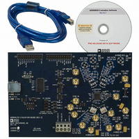
BOARD EVALUATION FOR AD9958
Manufacturer
Analog Devices Inc
Datasheet
1.AD9958BCPZ.pdf
(44 pages)
Specifications of AD9958/PCB
Design Resources
Low Jitter Sampling Clock Generator for High Performance ADCs Using AD9958/9858 and AD9515 (CN0109) Phase Coherent FSK Modulator (CN0186)
Lead Free Status / RoHS Status
Contains lead / RoHS non-compliant
Available stocks
Company
Part Number
Manufacturer
Quantity
Price
Company:

Part Number:
AD9958/PCBZ
Manufacturer:
Analog Devices Inc
Quantity:
135


AD9958
TABLE OF CONTENTS
Features .............................................................................................. 1
Applications ....................................................................................... 1
Functional Block Diagram .............................................................. 1
General Description ......................................................................... 3
Specifications ..................................................................................... 4
Absolute Maximum Ratings ............................................................ 8
Pin Configuration and Function Descriptions ............................. 9
Typical Performance Characteristics ........................................... 11
Application Circuits ....................................................................... 14
Equivalent Input and Output Circuits ......................................... 17
Theory of Operation ...................................................................... 18
Modes of Operation ....................................................................... 19
REVISION HISTORY
7/08—Rev. 0 to Rev. A
Changes to Features .......................................................................... 1
Inserted Figure 1; Renumbered Sequentially ................................ 1
Changes to Input Level Parameter in Table 1 ............................... 4
Added Profile Pin Toggle Rate Parameter in Table 1 ................... 6
Changes to Layout ............................................................................ 8
Changes to Table 3 ............................................................................ 9
Added Equivalent Input and Output Circuits Section .............. 17
Changes to Reference Clock Input Circuitry Section ................ 20
Change to Figure 35 ....................................................................... 21
Changes to Setting the Slope of the Linear Sweep Section ....... 25
Changes to Figure 37 ...................................................................... 26
Changes to Figure 38 and Figure 39 ............................................. 27
Changes to Figure 40 ...................................................................... 30
ESD Caution .................................................................................. 8
DDS Core ..................................................................................... 18
Digital-to-Analog Converter .................................................... 18
Channel Constraint Guidelines ................................................ 19
Power Supplies ............................................................................ 19
Single-Tone Mode ...................................................................... 19
Reference Clock Modes ............................................................. 20
Scalable DAC Reference Current Control Mode ................... 21
Power-Down Functions ............................................................. 21
Modulation Mode ....................................................................... 21
Modulation Using SDIO_x Pins for RU/RD........................... 24
Rev. A | Page 2 of 44
Synchronizing Multiple AD9958 Devices ................................... 29
Serial I/O Port ................................................................................. 31
Register Maps and Bit Descriptions ............................................. 36
Outline Dimensions ....................................................................... 44
Added Table 25; Renumbered Sequentially ................................ 31
Changes to Figure 41 ...................................................................... 31
Changes to Figure 42, Serial Data I/O (SDIO_0, SDIO_1,
SDIO_3) Section, and Added Example Instruction Byte
Section .............................................................................................. 32
Added Table 27 ............................................................................... 33
Changes to Figure 46, Figure 47, Figure 48, and Figure 49....... 35
Changes to Register Maps and Bit Descriptions Section and
Added Endnote 2 to Table 28 ........................................................ 36
Added Endnote 1 to Table 30 ........................................................ 38
Added Exposed Pad Notation to Outline Dimensions ............. 44
9/05—Revision 0: Initial Version
Linear Sweep Mode .................................................................... 25
Linear Sweep No-Dwell Mode ................................................. 26
Sweep and Phase Accumulator Clearing Functions .............. 27
Output Amplitude Control Mode ............................................ 28
Automatic Mode Synchronization ........................................... 29
Manual Software Mode Synchronization ................................ 29
Manual Hardware Mode Synchronization .............................. 29
I/O_UPDATE, SYNC_CLK, and System Clock
Relationships ............................................................................... 30
Overview ..................................................................................... 31
Instruction Byte Description .................................................... 32
Serial I/O Port Pin Description ................................................ 32
Serial I/O Port Function Description ...................................... 32
MSB/LSB Transfer Description ................................................ 32
Serial I/O Modes of Operation ................................................. 33
Register Maps .............................................................................. 36
Descriptions for Control Registers .......................................... 39
Descriptions for Channel Registers ......................................... 41
Ordering Guide .......................................................................... 44
Related parts for AD9958/PCB
Image
Part Number
Description
Manufacturer
Datasheet
Request
R

Part Number:
Description:
BOARD EVALUATION FOR AD9958
Manufacturer:
Analog Devices Inc
Datasheet:


Part Number:
Description:
±1.7g Dual-Axis IMEMS Accelerometer Evaluation Board
Manufacturer:
Analog Devices Inc
Datasheet:

Part Number:
Description:
Inertial Sensor Evaluation System
Manufacturer:
Analog Devices Inc
Datasheet:
Part Number:
Description:
Manufacturer:
Analog Devices Inc
Datasheet:
Part Number:
Description:
Manufacturer:
Analog Devices Inc
Datasheet:
Part Number:
Description:
Manufacturer:
Analog Devices Inc
Datasheet:
Part Number:
Description:
Manufacturer:
Analog Devices Inc
Datasheet:
Part Number:
Description:
Manufacturer:
Analog Devices Inc
Datasheet:
Part Number:
Description:
Manufacturer:
Analog Devices Inc
Datasheet:
Part Number:
Description:
Manufacturer:
Analog Devices Inc
Datasheet:
Part Number:
Description:
Manufacturer:
Analog Devices Inc
Datasheet:
Part Number:
Description:
Manufacturer:
Analog Devices Inc
Datasheet: