AD8364-EVAL-2140 Analog Devices Inc, AD8364-EVAL-2140 Datasheet
AD8364-EVAL-2140
Specifications of AD8364-EVAL-2140


Related parts for AD8364-EVAL-2140


AD8364-EVAL-2140 Summary of contents
Page 1
... OUTP and OUTN. An optional voltage applied to VLVL provides a common mode reference level to offset OUTP and OUTN above ground. The AD8364 is supplied in a 32-lead × LFCSP, for the operating temperature of –40°C to +85°C. One Technology Way, P.O. Box 9106, Norwood, MA 02062-9106, U.S.A. ...
Page 2
... AD8364 TABLE OF CONTENTS Specifications..................................................................................... 3 Absolute Maximum Ratings............................................................ 7 ESD Caution.................................................................................. 7 Pin Configuration and Function Descriptions............................. 8 Typical Performance Characteristics ............................................. 9 General Description and Theory.................................................. 18 Square Law Detector and Amplitude Target .......................... 19 RF Input Interface ...................................................................... 19 Offset Compensation ................................................................. 19 Temperature Sensor Interface................................................... 20 VREF Interface ........................................................................... 20 Power-Down Interface............................................................... 20 VST[A, B] Interface.................................................................... 20 OUT[ Outputs ...
Page 3
... PINHB = −50 dBm, OUTA = OUTA ± PINHA = −40 dBm and −20 dBm, INH[ 25°C, balun = Mini-Circuits® JTX-4-10T < +85°C A < +85° −10 dBm INH[ −40 dBm INH[A, B] Rev Page AD8364 Min Typ Max Unit LF 2.7 GHz 2 nV/√ 62/59 ...
Page 4
... AD8364 Parameter Conditions Temperature Sensitivity Deviation from OUT[ 25°C −40°C < T −40°C < T −40°C < T Deviation from OUTP to OUTN @ 25°C −40°C < T −40°C < T −40°C < T Input A to Input B Isolation Baluns = Macom ETC1.6-4-2-3 (both channels) ...
Page 5
... A INH[ −50 dBm, OUTB = OUTB ± PINHB = −50 dBm, OUTA = OUTA ± PINHA ≥ 200 Ω to ground ≥ 200 Ω to ground / change S Rev Page AD8364 Min Typ Max Unit 0.90 V +0.1, −0.4 dB +0.1, −0.4 dB +0.1, −0.4 dB +0.1, −0.4 dB +0.2, − ...
Page 6
... AD8364 Parameter Conditions SETPOINT INPUT Pin VSTA and VSTB Voltage Range Law conformance error ≤1 dB Input Resistance Logarithmic Scale Factor f = 450 MHz, −40°C ≤ T Logarithmic Intercept f = 450 MHz, −40°C ≤ T CHANNEL DIFFERENCE OUTPUT Pin OUTP and OUTN Voltage Range Min ...
Page 7
... This is a stress rating only; functional operation of the device at these or any other conditions above those indicated in the operational section of this specification is not implied. Exposure to absolute maximum rating conditions for extended periods may affect device reliability Rev Page AD8364 ...
Page 8
... INHA, INLA Channel A High and Low RF Signal Input Terminal. 28 PWDN Disable/Enable Control Input. Apply logic high voltage to shut down the AD8364. 30, 31 INLB, INHB Channel B Low and High RF Signal Input Terminal. Under Exposed Paddle The exposed paddle on the under side of the package should be soldered to a ground plane Package with low thermal and electrical characteristics ...
Page 9
... POLARITY AND MAGNITUDE OF THE DEVIATION APPLIED TO THE INHA INPUT, RELATIVE TO THE INLA INPUT, –2DB AS REFERENCED TO THE REF SIGNAL. –40 –35 –30 –25 –20 –15 –10 –5 RF INPUT AT INLA (dBm) Differential Drive AD8364 2.5 2.0 1.5 1.0 0.5 0 –0.5 –1.0 –1.5 –2.0 –2 2.5 2 ...
Page 10
... AD8364 –60 –50 –40 –30 –20 –10 INPUT AMPLITUDE (dBm) Figure 9. OUT[A, B] Voltage and Log Conformance vs. Input Amplitude at 880 MHz, Typical Device, ADJ[ 0.5 V, Sine Wave, Differential Drive, Balun = Mini-Circuits JTX-4-10T –60 –50 –40 –30 –20 –10 INPUT AMPLITUDE (dBm) Figure 10. Distribution of OUT[A, B] Voltage and Error over Temperature After Ambient Normalization vs ...
Page 11
... AND MAGNITUDE OF THE DEVIATION APPLIED TO THE INHA INPUT, RELATIVE TO THE INLA INPUT, AS REFERENCED TO THE REF SIGNAL. –35 –30 –25 –20 –15 –10 – INPUT AT INLA (dBm) Sine Wave, Differential Drive AD8364 2.5 2.0 1.5 1.0 0.5 0 –0.5 –1.0 –1.5 –2.0 –2 ...
Page 12
... AD8364 –60 –50 –40 –30 –20 –10 INPUT AMPLITUDE (dBm) Figure 21. OUT[A, B] Voltage and Log Conformance vs. Input Amplitude at 2.14 GHz, Typical Device, ADJ[ 0.85 V, Sine Wave, Differential Drive, Balun = Murata LDB212G1020C-001 –60 –50 –40 –30 –20 –10 INPUT AMPLITUDE (dBm) Figure 22. Distribution of OUT[A, B] Voltage and Error over Temperature After Ambient Normalization vs ...
Page 13
... SERIES NAME INDICATES THE POLARITY AND MAGNITUDE OF THE DEVIATION APPLIED TO THE INHA INPUT, RELATIVE TO THE INLA INPUT, AS REFERENCED TO THE REF SIGNAL. –35 –30 –25 –20 –15 –10 – INPUT AT INLA (dBm) Differential Drive AD8364 2.5 2.0 1.5 1.0 0.5 0 –0.5 –1.0 –1.5 –2.0 –2 ...
Page 14
... AD8364 2.0 1.5 ERROR CW ERROR QPSK 4dB CF 1.0 ERROR 256 QAM 8dB CF 0.5 0 –0.5 ERROR 16C CDMA2K –1.0 9CH SR1 14dB CF –1.5 ERROR 1C TM1-32 DPCH 13dB CF –2.0 –60 –55 –50 –45 –40 –35 –30 –25 –20 –15 –10 – MEAS (dBm) IN Figure 33 ...
Page 15
... TEMPERATURE (°C) Figure 40. Change in VREF vs. Temperature for 11 Devices 450MHz, 0dB 450MHz, –40dB 450MHz, –20dB 2140MHz, –20dB 2140MHz, –40dB 2140MHz, 0dB 450MHz, RF OFF 450MHz 1k 10k 100k 1M FREQUENCY (Hz) 0dB –20dB –40dB RF OFF 100 1k 10k 100k 1M FREQUENCY (Hz) Frequency = 2140 MHz AD8364 10M 10M ...
Page 16
... AD8364 10000 0dB 1000 –20dB –40dB 100 RF OFF 10 100 1k 10k 100k FREQUENCY (Hz) Figure 43. Noise Spectral Density of OUT[A, B]; CLP[ 0.1 µF, Frequency = 2140 MHz RF BURST ENABLE 2 OUTA CARRIER FREQUENCY 450MHz, CLPA = OPEN 0dBm –20dBm –40dBm B2 CH2 5.0V M2.0µs 1.25GS/s CH4 1.0V A CH2 2 ...
Page 17
... Figure 48. Output Voltage Stability vs. VP (Supply Voltage) at 2.14 GHz, When VP Varies by 10%,ADJ[A, B] =0.85 V, Sine Wave, Differential Drive, Murata LDB212G1020C-001 1 Rev Page PWDN INCREASING V PWDN DECREASING 1.2 1.4 1.6 1.8 2.0 2.2 V (V) PWDN Figure 49. Supply Current vs. V PWDN AD8364 2.4 ...
Page 18
... The device accurately measures waveforms that have a high peak-to-rms ratio (crest factor). Figure 50 shows a block diagram. A single channel of the AD8364 consists of a high performance AGC loop. As shown in Figure 51, the AGC loop comprises a wide bandwidth variable gain amplifier (VGA), square law detectors, an amplitude target circuit, and an output driver ...
Page 19
... The RF feedback signal to the input pins is forced to have an rms value determined by VSTA or VSTB. RF INPUT INTERFACE The AD8364’s RF inputs are connected as shown in Figure 52. There are 100 Ω resistors connected between DEC[A, B] and INH[A, B] and also between DEC[A, B] and INL[A, B]. The DEC[A, B] pins have a dc level established as (7 × ...
Page 20
... COMR Figure 54. VREF Interface Simplified Schematic POWER-DOWN INTERFACE The operating and stand-by currents for the AD8364 at 25°C are approximately 70 mA and 500 µA, respectively. The PWDN pin is connected to an internal resistor divider made with two 42 kΩ resistors. The divider voltage is applied to the base of an NPN transistor to force a power-down condition when the device is active ...
Page 21
... OUT[ OUTPUTS The output drivers used in the AD8364 are different than the output stage on the AD8362. The AD8364 incorporates rail-to- rail output drivers with pull-up and pull-down capabilities. The output noise is approximately 40 nV/√Hz at 100 kHz. OUT[ can source and sink mA. There is also an internal load from both OUTA and OUTB to ACOM of 2.5 kΩ ...
Page 22
... ADC connection. CONTROLLER MODE The channel difference outputs can be used for controlling a feedback loop to the AD8364’s RF inputs. A capacitor connected between FBKA and OUTP forms an integrator, keeping in mind that the on-chip 1 kΩ feedback resistor forms a zero. (The value of the on-chip resistors can vary as much as ± ...
Page 23
... The input signals are applied to the input differentially. The RF inputs of the AD8364 have a differential input impedance of 200 Ω. When the AD8364 RF inputs are driven from a 50 Ω source, a 4:1 balun transformer is recommended to provide the necessary impedance transformation. The inputs can be driven ...
Page 24
... If the gain control sense of the VGA is positive, an inverting op amp circuit with a dc offset shift can be used between the AD8364 and the VGA to keep the gain control voltage in the range. VSTA becomes the setpoint input to the system. This can be ...
Page 25
... TO 3.5V Figure 61. Operation in Controller Mode for Automatic Power Control Automatic Gain Control Figure 62 shows how the AD8364 can be connected to provide automatic gain control to an amplifier or signal chain. Additional pins are omitted for clarity. In this configuration, both rms detectors are connected in measurement mode with appropriate filtering being used on CLP[ effect a valid rms computation on both channels ...
Page 26
... I ERR VGA CONTROL 2 I INHA CHANNEL A SIG TruPwr™ INLA 2 I TGT OUTA AD8364 OUTB INLB 2 I CHANNEL B SIG INHB TruPwr™ TGT VGA CONTROL VLVL Figure 62. Operation in Controller Mode for Automatic Gain Control Rev Page DIRECTIONAL ...
Page 27
... Using this configuration, the RF input signal is down converted to 80 MHz using the AD8343 and amplified using the AD8367. The signal then splits and part fed back to the AD8364 through Channel B, and a setpoint voltage is applied to VSTB. This voltage corresponds to a particular power level, which is determined by the slope of the AD8364 ...
Page 28
... C8 C12 100pF 0.1µF SENSOR CHPA DECA COMA VPSR ACOM TEMP ACOM VPSA INHA INLA AD8364ACPZ PWDN COMR EXPOSED PADDLE INLB INHB VPSB CHPB DECB COMB ADJB ADJA VREF VLVL C19 C22 R20 R18 0.1µF 0.1µF 0Ω ...
Page 29
... Because the difference in the coupler values is 8.32 dB, a fixed gain of −8. expected. In practice, there is a gain of −13 dB. This is caused by the intercept shift of the AD8364 due to its frequency response, the insertion loss of the output coupler, and the insertion loss differences of the baluns used on the input of the AD8364 ...
Page 30
... C8 C12 100pF 0.1µF SENSOR CHPA DECA COMA VPSR ACOM TEMP ACOM VPSA INHA INLA AD8364 PWDN COMR INLB INHB VPSB CHPB DECB COMB ADJB ADJA VREF VLVL C19 C22 R20 R18 0.1µF 0.1µF 0Ω ...
Page 31
... Figure 68 shows a simplified schematic representation of the ADJ[A, B] interface. DEVICE CALIBRATION AND ERROR CALCULATION 2140 2500 The measured transfer function of the AD8364 at 2.14 GHz is 0.85 1.10 shown in Figure 69. The figure shows plots of both output voltage vs. input power and calculated error vs. input power. As the input power varies from − ...
Page 32
... These points are at the end of the device’s linear range. At 25°C, there is an error the calibration points. Note also that the range over which the AD8364 maintains an error of <±0 extended 25°C. The disadvantage of this approach is that linearity suffers, )/Slope especially at the top end of the input range ...
Page 33
... Rev Page ERROR CW –40°C ERROR CW +25°C ERROR CW +85°C 0 –60 –55 –50 –45 –40 –35 –30 –25 –20 –15 –10 –5 P MEAS (dBm) IN AD8364 2.0 1.6 1.2 0.8 0.4 0 –0.4 –0.8 –1.2 –1.6 –2 ...
Page 34
... Operating at a high slope is useful when it is desired to measure a particular section of the input range in greater detail. A measurement range would correspond change in VOUT at this slope, exceeding the capacity of the AD8364’s output stage when operating supply. This requires that the intercept is repositioned to place the desired input range section within a window corresponding to an output range of 0.1 V ≤ ...
Page 35
... When isolation is a concern useful to adjust the input power so the lowest expected detectable power is not far from the lowest detectable power of the AD8364 at the frequency of operation. The AD8364’s lowest detectable power point has little variation from part to part and is not affected by the balun ...
Page 36
... CLP[A, B]. Once the response time is set so that the AD8364 is just able to follow the RF burst requirements (within the tolerance of the capacitors), the output of the AD8364 should be evaluated with an oscilloscope ...
Page 37
... PRINTED CIRCUIT BOARD CONSIDERATIONS Each RF input pin of the AD8364 presents 100 Ω impedance relative to their respective ac grounds. To ensure that signal integrity is not seriously impaired by the printed circuit board (PCB), the relevant connection traces should provide appropriate characteristic impedance to the ground plane. This can be achieved through proper layout ...
Page 38
... Other selected configurations are shown in Figure 82 and Figure 83 as well. SIGNAL INA –3dB SOURCE AD8364 CHARACTERIZATION BOARD SIGNAL INB –3dB SOURCE COMPUTER CONTROLLER Figure 81 ...
Page 39
... VPOS R24 0Ω C13 R5 0.1µF 0Ω C8 C12 0.1µF 100pF C15 CLPA DECA COMA VPSR ACOM TEMP ACOM CLPA VSTA OUTA FBKA AD8364ACPZ OUTP OUTN FBKB OUTB VSTB DECB COMB ADJB ADJA VREF VLVL CLPB C16 CLPB C24 100pF AD8364 ...
Page 40
... CIRCUIT BOARD LAYOUTS There are two evaluation boards for the AD8364, one appropriate for low frequency work (AD8364-EVAL-500) and another one designed for use at 2140 MHz (AD8364-EVAL- 2140). Each board has a balun specific to operation in the designated frequency range. The RF area layout of the circuit ...
Page 41
... Figure 85. AD8364_EVAL-2140 Evaluation Board RF Area Layout Figure 86. 880 MHz Characterization Board RF Area Layout Rev Page AD8364 ...
Page 42
... AD8364 Table 7. AD8364-EVAL-500 Evaluation Board Configuration Options (10 MHz to 650 MHz) Component Function/Notes T1, T2 The dynamic range of the AD8364 is directly related to the magnitude and phase balance of the balun feeding the RF signal to the part. The evaluation board includes M/A-COM ETK4-2T soldered to the board and two unsoldered M/A-COM ETC1 ...
Page 43
... Table 7. AD8364-EVAL-2140 Evaluation Board Configuration Options (2140 MHz) Component Function/Notes T1, T2 The dynamic range of the AD8364 is directly related to the magnitude and phase balance of the balun feeding the RF signal to the part. At 2140 MHz, we have found it necessary to use a narrow band balun and have used the Murata LDB212G1020C-001 ...
Page 44
... OPEN OPEN R19 R17 R16 C24 0Ω 0Ω OPEN 100pF SW6 SW5 SW4 A VREF ADJB ADJA J13 J12 Figure 87. AD8364-EVA-500 Evaluation Board Rev Page C14 R6 TEMP 0Ω J4 C15 0.1µ CLPA B SW2 VSTA 0Ω OUTA 15 R10 0Ω FBKA 14 ...
Page 45
... R17 R16 0Ω 0Ω OPEN SW6 SW5 SW4 A B VREF ADJB ADJA REF LEVEL J13 J12 VOLTAGE J11 Figure 88. AD8364-EVAL-2140 Evaluation Board Rev Page AD8364 R6 0Ω VREF C15 0.1µF R27 SETPOINT VOLTAGE A OPEN J5 B SW2 0Ω OUTPUT 15 VOLTAGE A J6 R10 0Ω ...
Page 46
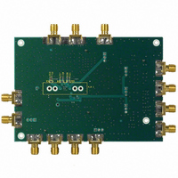
... AD8364 ASSEMBLY DRAWINGS Figure 89. AD8364-EVAL-500 Assembly Drawing Figure 90. AD8364-EVAL-2140 Assembly Drawing Rev Page ...
Page 47
... ORDERING GUIDE Model Temperature Range 1, 2 AD8364ACPZ-WP −40°C to +85°C AD8364ACPZ-REEL7 1 −40°C to +85°C 1 AD8364ACPZ-RL2 −40°C to +85°C AD8364ACP-REEL7 −40°C to +85°C AD8364-EVAL-500 AD8364-EVAL-2140 Pb-free part Waffle Pack 5.00 BSC SQ 0.60 MAX 24 0.50 BSC TOP 4.75 VIEW BSC SQ ...
Page 48
... AD8364 NOTES © 2005 Analog Devices, Inc. All rights reserved. Trademarks and registered trademarks are the property of their respective owners. D05334–0–4/05(0) Rev Page ...