CDB5571-2 Cirrus Logic Inc, CDB5571-2 Datasheet
CDB5571-2
Specifications of CDB5571-2


Related parts for CDB5571-2


CDB5571-2 Summary of contents
Page 1
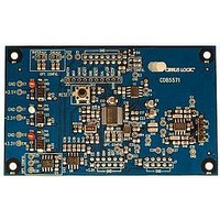
... Evaluation Board General Description The CDB5571 is a versatile tool designed for evaluating the func- tionality and performance of the CS5571 ADC (Analog-to-Digital Converter). The SPI serial port on the CDB5571 evaluation board is configured in Master mode and will start transmitting data after power-up upon reset ...
Page 2
... A.2 Hardware Considerations .................................................................................................. 9 APPENDIX B. BILL OF MATERIALS ........................................................................................ 10 APPENDIX C. SCHEMATICS ..................................................................................................... 11 APPENDIX D. LAYER PLOTS ................................................................................................... 16 APPENDIX E. CALIBRATION FUNCTION ................................................................................. 25 APPENDIX E. REVISION HISTORY .......................................................................................... 26 Figure 1. CDB5571 Block Diagram ................................................................................................. 4 Figure 2. CDB5571 Board Layout ................................................................................................... 5 Figure 3. Schematic - Block Diagram............................................................................................ 11 Figure 4. Schematic - Power Supplies .......................................................................................... 12 Figure 5. Schematic - Input Buffers and Multiplexer ..................................................................... 13 Figure 6. Schematic - CS5571 ...................................................................................................... 14 Figure 7. Schematic - Configuration & ...
Page 3
... CS5571. Interfacing the CDB5571 evaluation board to a user-supplied data capture system can be as simple as connecting the SPI port and using the CDB5571 default hardware configuration. In this config- uration, simply press the Reset switch on the CDB5571 and it will automatically begin transmitting data to the data capture system. ...
Page 4
... Overview The CDB5571 evaluation board has both analog and digital circuit sections. The analog section consists of the CS5571 ADC, two analog input signal buffers, controlled through a multiplexer, that condition the signals into the ADC, and a precision 4.096 V reference. The digital section consists of board operation configuration control signals, reset circuitry, an SPI™ ...
Page 5
... Connect the analog input signal source to the evaluation board per Table 2 on page 6. Verify from Table 4 on page 8 that the analog input channel selected is IN_A. 5. Configure the CDB5571 by connecting the control signal sources to the evaluation board as shown in Table 3 on page 7. Apply logic-level inputs as required to override the resistor pull-ups/pull-downs. ...
Page 6
... HARDWARE DESCRIPTION 3.1 Absolute Maximum Ratings Observe the following limits to ensure the CDB5571 component ratings are not exceeded. • CS5571 – The absolute maximum supply voltage that can be applied to the +3.3V power supply connection is +3.6V. – The absolute maximum power supply voltage that can be applied between pins VL and V1- is 6.1 V. • ...
Page 7
... Voltage Reference The voltage reference IC provided generates a 4.096 V precision reference. 3.3.5 ADC Reference Frequency The reference frequency for the CS5571 ADC is provided by a 16.000 MHz oscillator. DS768DB4 Table 3. Analog Input Channel Selection Multiplexer Input Channel Enabled 0 V 3.3 V CDB5571 ...
Page 8
... Digital Section 3.4.1 Hardware Configuration The CDB5571 evaluation board hardware comes pre-configured so the only connection required between it and a data acquisition system is the serial port connection. The hardware setup is reconfigurable through the hardware control interface connectors. Configure the evaluation board by setting the appropriate control line to the appropriate logic level. ...
Page 9
... Minimize ADC digital output edge transition current loading. A.2 Hardware Considerations At a system level, use shielded cable for interconnects. Keep interconnect cable lengths as short as pos- sible. Route analog and digital signals connecting to the PCB away from each other. DS768DB4 CDB5571 9 ...
Page 10
... APPENDIX B. BILL OF MATERIALS 10 CDB5571 DS768DB4 ...
Page 11
... APPENDIX C. SCHEMATICS DS768DB4 CDB5571 11 ...
Page 12
... CDB5571 DS768DB4 ...
Page 13
... DS768DB4 CDB5571 13 ...
Page 14
... CDB5571 DS768DB4 ...
Page 15
... DS768DB4 CDB5571 15 ...
Page 16
... APPENDIX D. LAYER PLOTS 16 CDB5571 DS768DB4 ...
Page 17
... DS768DB4 CDB5571 17 ...
Page 18
... CDB5571 DS768DB4 ...
Page 19
... DS768DB4 CDB5571 19 ...
Page 20
... CDB5571 DS768DB4 ...
Page 21
... DS768DB4 CDB5571 21 ...
Page 22
... CDB5571 DS768DB4 ...
Page 23
... DS768DB4 CDB5571 23 ...
Page 24
... CDB5571 DS768DB4 ...
Page 25
... APPENDIX E. CALIBRATION FUNCTION The calibration function has been removed from the CS5571. All references to calibration have been re- moved from this document. However, calibration still appears on the PCB. A jumper must be added to J2 for proper operation. DS768DB4 CDB5571 25 ...
Page 26
... SPI is a trademark of Motorola, Inc. PADS and PowerLogic are trademarks of Mentor Graphics. National Semiconductor is a registered trademark of National Semiconductor Corporation. 26 Changes Initial Release. Added 3.3.2 Mutiplexer section. Updated schematic to reflect new silicon revision. Removed calibration function / added Appendix E. CDB5571 DS768DB4 ...