ECJ-4YB1A226M Panasonic - ECG, ECJ-4YB1A226M Datasheet - Page 3
ECJ-4YB1A226M
Manufacturer Part Number
ECJ-4YB1A226M
Description
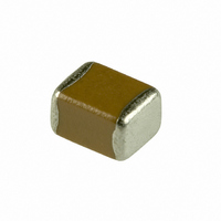
CAP 22UF 10V CERAMIC X5R 1210
Manufacturer
Panasonic - ECG
Series
ECJr
Datasheets
1.ECJ-RVB1H332M.pdf
(6 pages)
2.ECJ-RVB1H332M.pdf
(2 pages)
3.ECJ-RVB1H332M.pdf
(1 pages)
4.ECJ-RVB1H332M.pdf
(3 pages)
5.ECJ-0EB0J105K.pdf
(6 pages)
Specifications of ECJ-4YB1A226M
Capacitance
22µF
Voltage - Rated
10V
Tolerance
±20%
Temperature Coefficient
X5R
Mounting Type
Surface Mount, MLCC
Operating Temperature
-55°C ~ 85°C
Features
Low ESR
Applications
General Purpose
Package / Case
1210 (3225 Metric)
Size / Dimension
0.126" L x 0.098" W (3.20mm x 2.50mm)
Thickness
2.50mm
Lead Free Status / RoHS Status
Lead free / RoHS Compliant
Ratings
-
Lead Spacing
-
Other names
ECJ4YB1A226M
PCC2228TR
PCC2228TR


Design and specifi cations are each subject to change without notice. Ask factory for the current technical specifi cations before purchase and/or use.
Should a safety concern arise regarding this product, please be sure to contact us immediately.
Mixed mounting
with a component
with lead wires
Arrangement
near chassis
Retro-fi tting of
component with
lead wires
Lateral
arrangement
Prohibited Applications and Recommended Applications
2.3 Applications of Solder Resist
2.4 Component Layout
(a) Excessive amount (b) Proper amount
(2) The size of lands shall be designed to have equal
(1) Solder resist shall be utilized to equalize the amounts
(2) Solder resist shall be used to divide the pattern for the
The Capacitors/components shall be placed on the PC
board so as to have both electrodes subjected to uniform
stresses, or to position the component electrodes at right
angles to the grid glove or bending line. This should be
done to avoid cracking the Capacitors from bending of
the PC board after or during placing/mounting on the PC
board.
(1) To minimize mechanical stress caused by warp or
(2) The following drawing is for reference since
spacing between the right and left sides. If the
amount of solder on the right land is different from that
on the left land, the component may be cracked by
stress since the side with a larger amount of solder
solidifi es later during cooling.
of solder on both sides.
following cases;
Item
bending of a PC board, please follow the recommended
Capacitors’ layout below.
m e cha nic a l stress near the dividing/breaking
position of a PC board varies depending on the
mounting position of the Capacitors.
Prohibited layout
· Components are arranged closely.
· The Capacitor is mounted near a component with
· The Capacitor is placed near a chassis.
lead wires.
See the table below.
Recommended Amount of Solder
The lead wire of a component
Soldering iron
with lead wires
Land
Chassis
applications
Electrode pattern
Prohibited
Solder
(Ground solder)
A lead wire of
Retro-fitted component
Portion to be
excessively soldered
Layout the Capacitor sideways
against the stressing direction
Recommended layout
Improved applications
(c) Insufficient amount
by pattern division
Solder resist
Solder resist
Solder resist
Solder resist
– EC50 –
■ Precautions for Assembly
1. Storage
2. Adhesives for Mounting
2.5 Mounting Density and Spaces
(3) The magnitude of mechanical stress applied to the
If components are arranged in too narrow a space, the
components can be affected by solder bridges and
solder balls. The space between components should
be carefully determined.
(1) The Capacitors shall be stored between 5 - 40 °C
(2) If stored in a place that is humid, dusty, or contains
(3) Do not store components longer than 6 months.
(4) High dielectric constant capacitors (Class 2, characteristic
(5) When the initial capacitance is measured, the
(1) The amount and viscosity of an adhesive for mounting
(2) If the amount of adhesive is insuffi cient for mounting,
(3) If the adhesive is too low in its viscosity, the Capacitors
(4) Adhesives for mounting can be cured by ultraviolet
Capacitors when the circuit board is divided is in the
order of push back < slit < V-groove < perforation.
Also take into account the layout of the Capacitors
and the dividing/breaking method.
and 20 - 70 % RH, not under severe conditions of
high temperature and humidity.
corrosive gasses (hydrogen sulfi de, sulfurous acid,
hydrogen chloride and ammonia, etc.), the solderability
of the terminal electrodes may deteriorate.
In addition, storage in a place subjected to heating
and/or exposure to direct sunlight will causes
deformed tapes and reels, and component sticking to
tapes, both of which can result in mounting problems.
Check the solderability of products that have been
stored for more than 6 months before use.
B, X7R, X5R and F, Y5V) change in capacitance
with the passage of time, (Capacitance aging), due
to the inherent characteristics of ceramic dielectric
materials.
The capacitance change can be reversed to the initial
value at the time of shipping by heat treatment (See
1. Circuit Design, 1-7. Capacitance aging)
Capacitors shall be heat-treated at 150 +0/-10
°C for 1 hour and then subjected to ordinary
temperature and humidity for 48±4 hours before
measuring the initial values.
shall be such that the adhesive shall not fl ow off on
the land during its curing.
the Capacitor may fall off after or during soldering.
may be out of alignment after or during soldering.
or infrared radiation. In order to prevent the terminal
electrodes of the Capacitors from oxidizing, curing
shall be done under the following conditions: 160 °C
max., for 2 minutes max.
Perforation
Multilayer Ceramic Capacitors
Magnitude of stress A>B=C>D>E
A
E
C
Slit
D
B
00 Sep. 2008
Related parts for ECJ-4YB1A226M
Image
Part Number
Description
Manufacturer
Datasheet
Request
R

Part Number:
Description:
CAP ARRAY 10PF 50V NP0 1206
Manufacturer:
Panasonic - ECG
Datasheet:
Part Number:
Description:
CAP ARRAY 3300PF 50V X7R 1206
Manufacturer:
Panasonic - ECG
Datasheet:
Part Number:
Description:
CAP ARRAY 4700PF 50V X7R 1206
Manufacturer:
Panasonic - ECG
Datasheet:
Part Number:
Description:
CAP ARRAY 6800PF 50V X7R 1206
Manufacturer:
Panasonic - ECG
Datasheet:

Part Number:
Description:
CAP ARRAY 2200PF 50V X7R 0805
Manufacturer:
Panasonic - ECG
Datasheet:
Part Number:
Description:
CAP ARRAY 100PF 50V NP0 0805
Manufacturer:
Panasonic - ECG
Datasheet:
Part Number:
Description:
CAP ARRAY 47PF 50V NP0 0805
Manufacturer:
Panasonic - ECG
Datasheet:
Part Number:
Description:
CAP ARRAY 68PF 50V NP0 1206
Manufacturer:
Panasonic - ECG
Datasheet:
Part Number:
Description:
CAP ARRAY 150PF 50V NP0 1206
Manufacturer:
Panasonic - ECG
Datasheet:
Part Number:
Description:
CAP ARRAY .01UF 16V X7R 0805
Manufacturer:
Panasonic - ECG
Datasheet:


Part Number:
Description:
MICROPHONE OMNI 6X2.2MM W/CAP
Manufacturer:
Panasonic - ECG
Datasheet:

Part Number:
Description:
CAP .01UF 100V PEN FILM 1210 5%
Manufacturer:
Panasonic - ECG
Datasheet:

Part Number:
Description:
FILTER LINE 23.3MH 2A
Manufacturer:
Panasonic - ECG
Datasheet:

Part Number:
Description:
SAW FILTER PCS 1960 MHZ 50/150
Manufacturer:
Panasonic - ECG
Datasheet: