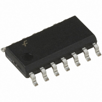
74LCX06M Fairchild Semiconductor, 74LCX06M Datasheet

74LCX06M
Specifications of 74LCX06M
Available stocks
Related parts for 74LCX06M
74LCX06M Summary of contents
Page 1
... Package Order Number Number 74LCX06M M14A 74LCX06SJ M14D 74LCX06MTC MTC14 Device also available in Tape and Reel. Specify by appending suffix letter “X” to the ordering number. All packages are lead free per JEDEC: J-STD-020B standard. Connection Diagram Pin Description Pin Names Description ...
Page 2
... CC V 2.7V–3. 2.3V–2. Free-Air Operating Temperature Input Edge Rate, V Note: 2. Unused inputs must be held HIGH or LOW. They may not float. ©1999 Fairchild Semiconductor Corporation 74LCX06 Rev. 1.8.0 Parameter (1) GND I (2) Parameter 0.8V–2.0V Rating –0.5V to +7.0V –0.5V to +7.0V – ...
Page 3
... OLP V Quiet Output Dynamic Valley V OLV Capacitance Symbol Parameter C Input Capacitance IN C Output Capacitance OUT C Power Dissipation Capacitance PD ©1999 Fairchild Semiconductor Corporation 74LCX06 Rev. 1.8.0 V (V) Conditions CC 2.3–2.7 2.7–3.6 2.3–2.7 2.7–3.6 2.3–3.6 I 100µA OL 2.3 I 8mA OL 2 ...
Page 4
... AC Loading and Waveforms Figure 1. AC Test Circuit (C 3-STATE Output Low Enable and Disable Times for Logic Figure 2. Waveforms (Input Characteristics 1MHz, t ©1999 Fairchild Semiconductor Corporation 74LCX06 Rev. 1.8.0 (Generic for LCX Family) includes probe and jig capacitance Symbol 3.3V ± 0.3V 2 ...
Page 5
... Package drawings are provided as a service to customers considering Fairchild components. Drawings may change in any manner without notice. Please note the revision and/or date on the drawing and contact a Fairchild Semiconductor representative to verify or obtain the most recent revision. Package specifications do not expand the terms of Fairchild’s worldwide terms and conditions, specifi ...
Page 6
... Package drawings are provided as a service to customers considering Fairchild components. Drawings may change in any manner without notice. Please note the revision and/or date on the drawing and contact a Fairchild Semiconductor representative to verify or obtain the most recent revision. Package specifications do not expand the terms of Fairchild’s worldwide terms and conditions, specifi ...
Page 7
... Package drawings are provided as a service to customers considering Fairchild components. Drawings may change in any manner without notice. Please note the revision and/or date on the drawing and contact a Fairchild Semiconductor representative to verify or obtain the most recent revision. Package specifications do not expand the terms of Fairchild’s worldwide terms and conditions, specifi ...
Page 8
... TRADEMARKS The following includes registered and unregistered trademarks and service marks, owned by Fairchild Semiconductor and/or its global subsidiaries, and is not intended exhaustive list of all such trademarks. ® ACEx Build it Now™ CorePLUS™ CROSSVOLT™ CTL™ Current Transfer Logic™ ...


