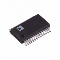
AD9214BRS-65 Analog Devices Inc, AD9214BRS-65 Datasheet

AD9214BRS-65
Specifications of AD9214BRS-65
Available stocks
Related parts for AD9214BRS-65
AD9214BRS-65 Summary of contents
Page 1
PRODUCT DESCRIPTION The AD9214 is a 10-bit monolithic sampling analog-to-digital converter (ADC) with an on-chip track-and-hold circuit, and is optimized for low cost, low power, small size, and ease of use. The product operates up to 105 MSPS conversion ...
Page 2
AD9214–SPECIFICATIONS ( DrV DD DC SPECIFICATIONS frequency used, unless otherwise noted.) Parameter Temp RESOLUTION ACCURACY No Missing Codes 25°C Full Offset Error Full 1 Gain Error 25°C 2 Differential Nonlinearity 25°C (DNL) Full 2 Integral Nonlinearity 25°C ...
Page 3
DIGITAL SPECIFICATIONS Parameter Temp 1 DIGITAL INPUTS Logic “1” Voltage Full Logic “0” Voltage Full Input Capacitance Full 2 DIGITAL OUTPUTS Logic Compatibility Logic “1” Voltage Full Logic “0” Voltage Full NOTES 1 Digital Inputs include ENCODE and PWRDN. 2 ...
Page 4
AD9214–SPECIFICATIONS SWITCHING SPECIFICATIONS Parameter Temp ENCODE INPUT PARAMETERS Maximum Conversion Rate Full Minimum Conversion Rate Full Encode Pulsewidth High (t ) Full EH Encode Pulsewidth Low (t ) Full EL Aperture Delay (t ) 25°C A Aperture Uncertainty (Jitter) 25°C ...
Page 5
... Typical thermal impedances (package = 28 SSOP); θ 2 measurements were taken on a 6-layer board in still air with a solid ground plane. Model Temperature Range AD9214BRS-65 –40°C to +85°C (Ambient) AD9214BRS-80 –40°C to +85°C (Ambient) AD9214BRS-105 –40°C to +85°C (Ambient) AD9214-65PCB 25° ...
Page 6
AD9214 Pin No. Mnemonic Function 1 OR CMOS Output; Out-of-Range Indicator. Logic HIGH indicates the analog input voltage was outside the converter’s range for the current output data. 2 DFS/GAIN Data Format Select and Gain Mode Select. Connect externally to ...
Page 7
TERMINOLOGY Analog Bandwidth The analog input frequency at which the spectral power of the fundamental frequency (as determined by the FFT analysis) is reduced by 3 dB. Aperture Delay The delay between the 50% point of the rising edge of ...
Page 8
AD9214 Transient Response Time Transient response is defined as the time it takes for the ADC to reacquire the analog input after a transient from 10% above negative full scale to 10% below positive full scale. EQUIVALENT CIRCUITS 30k 40 ...
Page 9
ENCODE: 105MSPS A : 50.3MHz @ –0.5dBFS –10 IN SNR: 53.0dB ENOB: 8.5 BITS –20 SFDR: 64dBFS –30 –40 –50 –60 –70 –80 –90 –100 0 FREQUENCY – MHz 0 ENCODE: 80MSPS A : 70.3MHz @ –0.5dBFS –10 IN ...
Page 10
AD9214 100 90 2ND 80 3RD 70 SFDR FREQUENCY – MHz 0 ENCODE: 80MSPS A : 29.3MHz @ –6dBFS –10 IN 30.3MHz @ –6dBFS SFDR: 74dBFS –20 –30 –40 –50 –60 –70 –80 –90 ...
Page 11
SNR 10.3MHz/105MSPS 54 SINAD 10.3MHz/105MSPS – TEMPERATURE – C 4.0 3.5 3.0 2.5 2.0 1.5 1.0 0.5 0.0 – TEMPERATURE – C 1.240 1.235 1.230 1.225 1.220 –40 0 ...
Page 12
AD9214 THEORY OF OPERATION The AD9214 architecture is a bit-per-stage pipeline converter utilizing switch capacitor techniques. These stages determine the 7 MSBs and drive a 3-bit flash. Each stage provides suffi- cient overlap and error correction allowing optimization of comparator ...
Page 13
AD8138 500 50 ANALOG + – SIGNAL VOCM SOURCE AV – 10k 500 500 5k 0.1 F POWER SUPPLIES The AD9214 has two power supplies, AV and AGND supply power to all the analog circuitry, ...
Page 14
AD9214 Reference Circuit The evaluation board is configured at assembly to use the AD9214’s on-board reference. To supply an external reference, the user must connect the REFSENSE pin to VCC by removing the jumper block connecting E25 to E26, and ...
Page 15
Quantity Reference Designator C1–C3, C5–C14, C16–C20, C25–C28 3 4 C21–C24 R1, R2, R4 R7, R10, R12, R17 7 4 U5– R21 9 2 R6, ...
Page 16
AD9214 ...
Page 17
AD9214 ...
Page 18
AD9214 0.078 (1.98) 0.068 (1.73) 0.008 (0.203) 0.002 (0.050) CONTROLLING DIMENSIONS ARE IN MILLIMETERS; INCH DIMENSIONS ARE ROUNDED-OFF MILLIMETER EQUIVALENTS FOR REFERENCE ONLY AND ARE NOT APPROPRIATE FOR USE IN DESIGN OUTLINE DIMENSIONS Dimensions shown in inches and (mm). 28-Lead ...
Page 19
Revision History Location Data Sheet changed from REV REV. D. Edit to Functional Block Diagram . . . . . . . . . . . . . . . . . . . . . . . ...
Page 20
...


