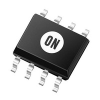
MC100EL01D ON Semiconductor, MC100EL01D Datasheet

MC100EL01D
Specifications of MC100EL01D
Available stocks
Related parts for MC100EL01D
MC100EL01D Summary of contents
Page 1
MC10EL01, MC100EL01 5V ECL 4‐Input OR/NOR Description The MC10EL/100EL01 is a 4-input OR/NOR gate. The device is functionally equivalent to the E101 device with higher performance capabilities. With propagation delays and output transition times significantly faster than the E101, the EL01 ...
Page 2
Table 1. PIN DESCRIPTION PIN D0− Table 2. MAXIMUM RATINGS Symbol Parameter V PECL Mode Power Supply CC V NECL Mode Power Supply EE V PECL Mode Input Voltage I NECL Mode Input ...
Page 3
Table 3. 10EL SERIES PECL DC CHARACTERISTICS Symbol Characteristic I Power Supply Current EE V Output HIGH Voltage (Note Output LOW Voltage (Note Input HIGH Voltage IH V Input LOW Voltage IL I Input ...
Page 4
Table 5. 100EL SERIES PECL DC CHARACTERISTICS Symbol Characteristic I Power Supply Current EE V Output HIGH Voltage (Note Output LOW Voltage (Note Input HIGH Voltage IH V Input LOW Voltage IL I Input ...
Page 5
... MC10EL01DG MC10EL01DR2 MC10EL01DR2G MC10EL01DT MC10EL01DTG MC10EL01DTR2 MC10EL01DTR2G MC10EL01MNR4 MC10EL01MNR4G MC100EL01D MC100EL01DG MC100EL01DR2 MC100EL01DR2G MC100EL01DT MC100EL01DTG MC100EL01DTR2 MC100EL01DTR2G MC100EL01MNR4 MC100EL01MNR4G †For information on tape and reel specifications, including part orientation and tape sizes, please refer to our Tape and Reel Packaging Specifications Brochure, BRD8011/ ...
Page 6
Resource Reference of Application Notes AN1405/D − ECL Clock Distribution Techniques AN1406/D − Designing with PECL (ECL at +5.0 V) AN1503/D − ECLinPSt I/O SPiCE Modeling Kit AN1504/D − Metastability and the ECLinPS Family AN1568/D − Interfacing Between LVDS and ...
Page 7
... G C SEATING PLANE −Z− 0.25 (0.010 *For additional information on our Pb−Free strategy and soldering details, please download the ON Semiconductor Soldering and Mounting Techniques Reference Manual, SOLDERRM/D. PACKAGE DIMENSIONS SOIC−8 NB CASE 751−07 ISSUE 0.10 (0.004 SOLDERING FOOTPRINT* 1 ...
Page 8
K 8x REF 0.10 (0.004) 0.15 (0.006 L −U− PIN 1 IDENT 0.15 (0.006 −V− C 0.10 (0.004) D −T− G SEATING PLANE PACKAGE DIMENSIONS TSSOP−8 ...
Page 9
... Opportunity/Affirmative Action Employer. This literature is subject to all applicable copyright laws and is not for resale in any manner. PUBLICATION ORDERING INFORMATION LITERATURE FULFILLMENT: Literature Distribution Center for ON Semiconductor P.O. Box 5163, Denver, Colorado 80217 USA Phone: 303−675−2175 or 800−344−3860 Toll Free USA/Canada Fax: 303− ...


