ESD5Z6.0T1G ON Semiconductor, ESD5Z6.0T1G Datasheet - Page 2
ESD5Z6.0T1G
Manufacturer Part Number
ESD5Z6.0T1G
Description
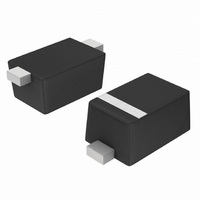
TVS ESD ASD 181W 6.0V SOD-523
Manufacturer
ON Semiconductor
Datasheet
1.ESD5Z5.0T1G.pdf
(4 pages)
Specifications of ESD5Z6.0T1G
Voltage - Reverse Standoff (typ)
6V
Voltage - Breakdown
6.8V
Power (watts)
181W
Polarization
Unidirectional
Mounting Type
Surface Mount
Package / Case
SOD-523
Number Of Elements
1
Polarity
Uni-Directional
Package Type
SOD-523
Operating Temperature Classification
Military
Reverse Breakdown Voltage
6.8V
Clamping Voltage
20.5V
Reverse Stand-off Voltage
6V
Leakage Current (max)
10nA
Peak Pulse Current
8.8A
Peak Pulse Power Dissipation
240W
Test Current (it)
1mA
Operating Temp Range
-55C to 150C
Mounting
Surface Mount
Pin Count
2
Channels
1 Channel
Operating Voltage
6 V
Breakdown Voltage
6.8 V
Termination Style
SMD/SMT
Peak Surge Current
8.8 A
Capacitance
70 pF
Maximum Operating Temperature
+ 150 C
Minimum Operating Temperature
- 55 C
Dimensions
0.8 mm W x 1.2 mm L
Lead Free Status / RoHS Status
Lead free / RoHS Compliant
Other names
ESD5Z6.0T1G
ESD5Z6.0T1GOSTR
ESD5Z6.0T1GOSTR
Available stocks
Company
Part Number
Manufacturer
Quantity
Price
Company:

Part Number:
ESD5Z6.0T1G
Manufacturer:
ON
Quantity:
150 000
Company:
Part Number:
ESD5Z6.0T1G
Manufacturer:
ON
Quantity:
30 000
Company:
Part Number:
ESD5Z6.0T1G
Manufacturer:
ON
Quantity:
30 000
Part Number:
ESD5Z6.0T1G
Manufacturer:
ON/安森美
Quantity:
20 000


* The “G'' suffix indicates Pb-Free package available.
**Other voltages available upon request.
†Surge current waveform per Figure 5.
2. V
3. For test procedure see Figures 3 and 4 and Application Note AND8307/D.
4. ESD5Z5.0T1G shown below. Other voltages available upon request.
ELECTRICAL CHARACTERISTICS
(T
*See Application Note AND8308/D for detailed explanations of
ELECTRICAL CHARACTERISTICS
ESD5Z2.5T1, G*
ESD5Z3.3T1, G*
ESD5Z5.0T1, G*
ESD5Z6.0T1, G*
ESD5Z7.0T1, G*
ESD5Z12T1, G*
Symbol
A
datasheet parameters.
V
V
P
= 25°C unless otherwise noted)
I
RWM
V
V
I
PP
I
I
C
BR
BR
R
Device**
T
F
pk
C
F
Figure 1. ESD Clamping Voltage Screenshot
is measured with a pulse test current I
Positive 8 kV contact per IEC 61000-4-2
Maximum Reverse Peak Pulse Current
Clamping Voltage @ I
Working Peak Reverse Voltage
Maximum Reverse Leakage Current @ V
Breakdown Voltage @ I
Test Current
Forward Current
Forward Voltage @ I
Peak Power Dissipation
Max. Capacitance @V
Marking
Device
ZG
ZM
ZD
ZE
ZF
ZH
V
Parameter
Max
RWM
2.5
3.3
5.0
6.0
7.0
(V)
12
F
PP
R
T
= 0 and f = 1 MHz
@ V
I
R
Max
0.05
0.05
0.01
0.01
0.01
(T
6.0
(mA)
RWM
A
T
= 25°C unless otherwise noted, V
at an ambient temperature of 25°C.
V
(Note 2)
BR
ESD5Z2.5T1 SERIES
RWM
@ I
14.1
Min
4.0
5.0
6.2
6.8
7.5
(V)
T
http://onsemi.com
mA
1.0
1.0
1.0
1.0
1.0
1.0
I
T
2
@ I
V
5.0 A
C
11.6
12.4
13.5
Typ
6.5
8.4
17
PP
(V)
†
=
Figure 2. ESD Clamping Voltage Screenshot
F
Negative 8 kV contact per IEC 61000-4-2
V
= 1.1 V Max. @ I
C
V
V
Max I
BR
C
Max
10.9
14.1
18.6
20.5
22.7
(V) @
25
V
PP
RWM
†
Uni-Directional TVS
F
Max
(A)
11.0
11.2
I
9.4
8.8
8.8
9.6
PP
= 10 mA for all types)
I
†
F
I
I
I
I
R
T
PP
(W)
Max
P
120
158
174
181
200
240
V
pk
F
†
(pF)
Typ
145
105
80
70
65
55
C
Figures 1 and 2
IEC61000-4-2
See Below
(Note 3)
(Note 4)
Per
V
V
C
Related parts for ESD5Z6.0T1G
Image
Part Number
Description
Manufacturer
Datasheet
Request
R

Part Number:
Description:
ON Semiconductor [VOLTAGE REGULATOR]
Manufacturer:
ON Semiconductor
Datasheet:
Part Number:
Description:
357-036-542-201 CARDEDGE 36POS DL .156 BLK LOPRO
Manufacturer:
ON Semiconductor
Datasheet:
Part Number:
Description:
357-036-542-201 CARDEDGE 36POS DL .156 BLK LOPRO
Manufacturer:
ON Semiconductor
Datasheet:
Part Number:
Description:
357-036-542-201 CARDEDGE 36POS DL .156 BLK LOPRO
Manufacturer:
ON Semiconductor
Datasheet:
Part Number:
Description:
357-036-542-201 CARDEDGE 36POS DL .156 BLK LOPRO
Manufacturer:
ON Semiconductor
Datasheet:
Part Number:
Description:
357-036-542-201 CARDEDGE 36POS DL .156 BLK LOPRO
Manufacturer:
ON Semiconductor
Datasheet:
Part Number:
Description:
357-036-542-201 CARDEDGE 36POS DL .156 BLK LOPRO
Manufacturer:
ON Semiconductor
Datasheet:
Part Number:
Description:
357-036-542-201 CARDEDGE 36POS DL .156 BLK LOPRO
Manufacturer:
ON Semiconductor
Datasheet:
Part Number:
Description:
357-036-542-201 CARDEDGE 36POS DL .156 BLK LOPRO
Manufacturer:
ON Semiconductor
Datasheet:
Part Number:
Description:
357-036-542-201 CARDEDGE 36POS DL .156 BLK LOPRO
Manufacturer:
ON Semiconductor
Datasheet:
Part Number:
Description:
357-036-542-201 CARDEDGE 36POS DL .156 BLK LOPRO
Manufacturer:
ON Semiconductor
Datasheet:
Part Number:
Description:
Manufacturer:
ON Semiconductor
Datasheet:
Part Number:
Description:
Manufacturer:
ON Semiconductor
Datasheet:
Part Number:
Description:
Manufacturer:
ON Semiconductor
Datasheet: