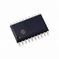
PIC18F13K22-I/SO Microchip Technology, PIC18F13K22-I/SO Datasheet - Page 244

PIC18F13K22-I/SO
Manufacturer Part Number
PIC18F13K22-I/SO
Description
IC MCU 8BIT 8KB FLASH 20SOIC
Manufacturer
Microchip Technology
Series
PIC® XLP™ 18Fr
Datasheets
1.PIC18LF13K22-ISS.pdf
(388 pages)
2.PIC18LF13K22-ISS.pdf
(12 pages)
3.PIC18F13K22-ISS.pdf
(382 pages)
Specifications of PIC18F13K22-I/SO
Program Memory Type
FLASH
Program Memory Size
8KB (4K x 16)
Package / Case
20-SOIC (7.5mm Width)
Core Processor
PIC
Core Size
8-Bit
Speed
64MHz
Connectivity
I²C, LIN, SPI, UART/USART
Peripherals
Brown-out Detect/Reset, POR, PWM, WDT
Number Of I /o
17
Eeprom Size
256 x 8
Ram Size
256 x 8
Voltage - Supply (vcc/vdd)
1.8 V ~ 5.5 V
Data Converters
A/D 12x10b
Oscillator Type
Internal
Operating Temperature
-40°C ~ 85°C
Processor Series
PIC18F
Core
PIC
Data Bus Width
8 bit
Data Ram Size
256 B
Interface Type
I2C, MSSP, SPI, USART
Maximum Clock Frequency
64 MHz
Number Of Programmable I/os
17
Number Of Timers
4
Operating Supply Voltage
1.8 V to 5.5 V
Maximum Operating Temperature
+ 125 C
Mounting Style
SMD/SMT
3rd Party Development Tools
52715-96, 52716-328, 52717-734, 52712-325, EWPIC18
Development Tools By Supplier
PG164130, DV164035, DV244005, DV164005
Minimum Operating Temperature
- 40 C
On-chip Adc
10 bit, 12 Channel
Package
20SOIC W
Device Core
PIC
Family Name
PIC18
Maximum Speed
64 MHz
A/d Bit Size
10 bit
A/d Channels Available
12
Height
2.05 mm
Length
12.8 mm
Supply Voltage (max)
5.5 V
Supply Voltage (min)
1.8 V, 2.7 V
Width
7.5 mm
Lead Free Status / RoHS Status
Lead free / RoHS Compliant
Lead Free Status / RoHS Status
Lead free / RoHS Compliant, Lead free / RoHS Compliant
Available stocks
Company
Part Number
Manufacturer
Quantity
Price
Company:
Part Number:
PIC18F13K22-I/SO
Manufacturer:
Microchip Technology
Quantity:
1 865
- Current page: 244 of 388
- Download datasheet (4Mb)
PIC18F1XK22/LF1XK22
20.2
The FVR is a stable fixed voltage reference,
independent of V
1.024V. This reference can be enabled by setting the
FVR1EN bit of the VREFCON0 register to ‘1’. The FVR
can be routed to the comparators or an ADC input
channel.
FIGURE 20-1:
DS41365D-page 244
V
FVR Reference Module
REF
V
REF
-
FVR1
+
V
DD
DD
, with a nominal output voltage of
D1PSS<1:0> = 01
VOLTAGE REFERENCE BLOCK DIAGRAM
D1PSS<1:0> = 10
D1PSS<1:0> = 00
D1LPS
D1EN
D1LPS
D1EN
D1NSS = 1
D1NSS = 0
32 Steps
Preliminary
R
R
R
R
R
R
R
R
FVR1S<1:0>
20.2.1
When the Fixed Voltage Reference module is enabled, it
will require some time for the reference and its amplifier
circuits to stabilize. The user program must include a
small delay routine to allow the module to settle. The
FVR1ST stable bit of the VREFCON0 register also
indicates that the FVR has been operating long enough
to
Specifications” for the minimum delay requirement.
FVR1EN
FVR1ST
DAC1R<4:0>
be
2
stable.
FVR STABILIZATION PERIOD
+
_
DAC1OE
See
X
X
X
1.024V Fixed
Reference
1
2
4
2010 Microchip Technology Inc.
Section 25.0
CV
REF
V
REF
pin
“Electrical
FVR
Related parts for PIC18F13K22-I/SO
Image
Part Number
Description
Manufacturer
Datasheet
Request
R

Part Number:
Description:
Manufacturer:
Microchip Technology Inc.
Datasheet:

Part Number:
Description:
Manufacturer:
Microchip Technology Inc.
Datasheet:

Part Number:
Description:
Manufacturer:
Microchip Technology Inc.
Datasheet:

Part Number:
Description:
Manufacturer:
Microchip Technology Inc.
Datasheet:

Part Number:
Description:
Manufacturer:
Microchip Technology Inc.
Datasheet:

Part Number:
Description:
Manufacturer:
Microchip Technology Inc.
Datasheet:

Part Number:
Description:
Manufacturer:
Microchip Technology Inc.
Datasheet:

Part Number:
Description:
Manufacturer:
Microchip Technology Inc.
Datasheet:


