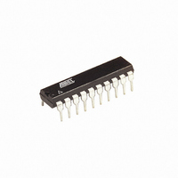
ATTINY2313-20PU Atmel, ATTINY2313-20PU Datasheet - Page 121

ATTINY2313-20PU
Manufacturer Part Number
ATTINY2313-20PU
Description
IC MCU AVR 2K FLASH 20DIP
Manufacturer
Atmel
Series
AVR® ATtinyr
Datasheets
1.ATTINY2313-20MU.pdf
(226 pages)
2.ATTINY2313V-10MU.pdf
(15 pages)
3.ATTINY2313V-10SU.pdf
(20 pages)
Specifications of ATTINY2313-20PU
Core Processor
AVR
Core Size
8-Bit
Speed
20MHz
Connectivity
SPI, UART/USART
Peripherals
Brown-out Detect/Reset, POR, PWM, WDT
Number Of I /o
18
Program Memory Size
2KB (1K x 16)
Program Memory Type
FLASH
Eeprom Size
128 x 8
Ram Size
128 x 8
Voltage - Supply (vcc/vdd)
2.7 V ~ 5.5 V
Oscillator Type
Internal
Operating Temperature
-40°C ~ 85°C
Package / Case
20-DIP (0.300", 7.62mm)
Package
20PDIP
Device Core
AVR
Family Name
ATtiny
Maximum Speed
20 MHz
Operating Supply Voltage
3.3|5 V
Data Bus Width
8 Bit
Number Of Programmable I/os
18
Interface Type
SPI/USART/USI
Number Of Timers
2
Processor Series
ATTINY2x
Core
AVR8
Data Ram Size
128 B
Maximum Clock Frequency
20 MHz
Maximum Operating Temperature
+ 85 C
Mounting Style
Through Hole
3rd Party Development Tools
EWAVR, EWAVR-BL
Development Tools By Supplier
ATAVRDRAGON, ATSTK500, ATSTK600, ATAVRISP2, ATAVRONEKIT
Minimum Operating Temperature
- 40 C
Cpu Family
ATtiny
Device Core Size
8b
Frequency (max)
20MHz
Total Internal Ram Size
128Byte
# I/os (max)
18
Number Of Timers - General Purpose
2
Operating Supply Voltage (typ)
3.3/5V
Operating Supply Voltage (max)
5.5V
Operating Supply Voltage (min)
2.7V
Instruction Set Architecture
RISC
Operating Temp Range
-40C to 85C
Operating Temperature Classification
Industrial
Mounting
Through Hole
Pin Count
20
Package Type
PDIP
For Use With
ATSTK600-DIP40 - STK600 SOCKET/ADAPTER 40-PDIP770-1007 - ISP 4PORT ATMEL AVR MCU SPI/JTAGATAVRDRAGON - KIT DRAGON 32KB FLASH MEM AVRATAVRISP2 - PROGRAMMER AVR IN SYSTEMATJTAGICE2 - AVR ON-CHIP D-BUG SYSTEM
Lead Free Status / RoHS Status
Lead free / RoHS Compliant
Data Converters
-
Lead Free Status / Rohs Status
Lead free / RoHS Compliant
Available stocks
Company
Part Number
Manufacturer
Quantity
Price
Part Number:
ATTINY2313-20PU
Manufacturer:
ATMEL/爱特梅尔
Quantity:
20 000
Data Reception –
The USART
Receiver
Receiving Frames with
5 to 8 Data Bits
2543L–AVR–08/10
The USART Receiver is enabled by writing the Receive Enable (RXEN) bit in the UCSRB Regis-
ter to one. When the Receiver is enabled, the normal pin operation of the RxD pin is overridden
by the USART and given the function as the Receiver’s serial input. The baud rate, mode of
operation and frame format must be set up once before any serial reception can be done. If syn-
chronous operation is used, the clock on the XCK pin will be used as transfer clock.
The Receiver starts data reception when it detects a valid start bit. Each bit that follows the start
bit will be sampled at the baud rate or XCK clock, and shifted into the Receive Shift Register until
the first stop bit of a frame is received. A second stop bit will be ignored by the Receiver. When
the first stop bit is received, i.e., a complete serial frame is present in the Receive Shift Register,
the contents of the Shift Register will be moved into the receive buffer. The receive buffer can
then be read by reading the UDR I/O location.
The following code example shows a simple USART receive function based on polling of the
Receive Complete (RXC) flag. When using frames with less than eight bits the most significant
bits of the data read from the UDR will be masked to zero. The USART has to be initialized
before the function can be used.
Note:
The function simply waits for data to be present in the receive buffer by checking the RXC flag,
before reading the buffer and returning the value.
Assembly Code Example
C Code Example
USART_Receive:
unsigned char USART_Receive( void )
{
}
; Wait for data to be received
sbis UCSRA, RXC
rjmp USART_Receive
; Get and return received data from buffer
in
ret
/* Wait for data to be received */
while ( !(UCSRA & (1<<RXC)) )
/* Get and return received data from buffer */
return UDR;
1. The example code assumes that the part specific header file is included.
For I/O Registers located in extended I/O map, “IN”, “OUT”, “SBIS”, “SBIC”, “CBI”, and “SBI”
instructions must be replaced with instructions that allow access to extended I/O. Typically
“LDS” and “STS” combined with “SBRS”, “SBRC”, “SBR”, and “CBR”.
r16, UDR
;
(1)
(1)
121


