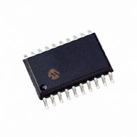
PIC24F08KA101-I/SO Microchip Technology, PIC24F08KA101-I/SO Datasheet - Page 57

PIC24F08KA101-I/SO
Manufacturer Part Number
PIC24F08KA101-I/SO
Description
IC PIC MCU FLASH 8K 20-SOIC
Manufacturer
Microchip Technology
Series
PIC® XLP™ 24Fr
Datasheets
1.MA240017.pdf
(254 pages)
2.PIC24F04KA201-ISS.pdf
(48 pages)
3.PIC24F16KA101-ISS.pdf
(18 pages)
Specifications of PIC24F08KA101-I/SO
Core Size
16-Bit
Program Memory Size
8KB (2.75K x 24)
Core Processor
PIC
Speed
32MHz
Connectivity
I²C, IrDA, SPI, UART/USART
Peripherals
Brown-out Detect/Reset, POR, PWM, WDT
Number Of I /o
18
Program Memory Type
FLASH
Eeprom Size
512 x 8
Ram Size
1.5K x 8
Voltage - Supply (vcc/vdd)
1.8 V ~ 3.6 V
Data Converters
A/D 9x10b
Oscillator Type
Internal
Operating Temperature
-40°C ~ 85°C
Package / Case
20-SOIC (7.5mm Width)
Controller Family/series
PIC24
No. Of I/o's
18
Eeprom Memory Size
512Byte
Ram Memory Size
1.5KB
Cpu Speed
32MHz
No. Of Timers
3
Core
PIC
Processor Series
PIC24F
Data Bus Width
16 bit
Maximum Clock Frequency
32 KHz
Data Ram Size
1.5 KB
On-chip Adc
10 bit, 9 Channel
Number Of Programmable I/os
18
Number Of Timers
3
Operating Supply Voltage
1.8 V to 3.6 V
Mounting Style
SMD/SMT
Height
2.05 mm
Interface Type
I2C, IrDA, SPI, UART
Length
12.8 mm
Maximum Operating Temperature
+ 125 C
Minimum Operating Temperature
- 40 C
Supply Voltage (max)
3.6 V
Supply Voltage (min)
1.8 V
Width
7.5 mm
Lead Free Status / RoHS Status
Lead free / RoHS Compliant
For Use With
MA240017 - MODULE PLUG-IN PIC24F16KA102 PIM
Lead Free Status / Rohs Status
Details
- Current page: 57 of 254
- Download datasheet (4Mb)
6.4.1.1
To erase the entire data EEPROM (bulk erase), the
address registers do not need to be configured
because this operation affects the entire data
EEPROM. The following sequence helps in performing
bulk erase:
1.
2.
3.
4.
5.
A typical bulk erase sequence is provided in
Example 6-3.
EXAMPLE 6-3:
EXAMPLE 6-4:
© 2009 Microchip Technology Inc.
int __attribute__ ((space(eedata))) eeData = 0x1234;
Configure NVMCON to Bulk Erase mode.
Clear NVMIF status bit and enable NVM
interrupt (optional).
Write the key sequence to NVMKEY.
Set the WR bit to begin erase cycle.
Either poll the WR bit or wait for the NVM
interrupt (NVMIF set).
int newData;
unsigned int offset;
// Set up NVMCON to erase one word of data EEPROM
NVMCON = 0x4004;
// Set up a pointer to the EEPROM location to be erased
TBLPAG = __builtin_tblpage(&eeData);
offset = __builtin_tbloffset(&eeData);
__builtin_tblwtl(offset, newData);
asm volatile ("disi #5");
__builtin_write_NVM();
// Set up NVMCON to bulk erase the data EEPROM
NVMCON = 0x4050;
// Disable Interrupts For 5 Instructions
asm volatile (“disi #5”);
// Issue Unlock Sequence and Start Erase Cycle
__builtin_write_NVM();
Data EEPROM Bulk Erase
DATA EEPROM BULK ERASE
SINGLE-WORD WRITE TO DATA EEPROM
Preliminary
PIC24F16KA102 FAMILY
6.4.2
To write a single word in the data EEPROM, the
following sequence must be followed:
1.
2.
3.
A typical single-word write sequence is provided in
Example 6-4.
// Variable located in EEPROM
// Initialize EE Data page pointer
// Initizlize lower word of address
// Write EEPROM data to write latch
// Disable Interrupts For 5 Instructions
// Issue Unlock Sequence & Start Write Cycle
// New data to write to EEPROM
Erase one data EEPROM word (as mentioned in
the
(NVMCON<12>) is set to ‘1’.
Write the data word into the data EEPROM
latch.
Program the data word into the EEPROM:
- Configure the NVMCON register to program one
- Clear NVMIF status bit and enable NVM
- Write the key sequence to NVMKEY.
- Set the WR bit to begin erase cycle.
- Either poll the WR bit or wait for the NVM
- To get cleared, wait until NVMIF is set.
EEPROM word (NVMCON<5:0> = 0001xx).
interrupt (optional).
interrupt (NVMIF set).
previous
SINGLE-WORD WRITE
section)
if
PGMONLY
DS39927B-page 55
bit
Related parts for PIC24F08KA101-I/SO
Image
Part Number
Description
Manufacturer
Datasheet
Request
R

Part Number:
Description:
Manufacturer:
Microchip Technology Inc.
Datasheet:

Part Number:
Description:
Manufacturer:
Microchip Technology Inc.
Datasheet:

Part Number:
Description:
Manufacturer:
Microchip Technology Inc.
Datasheet:

Part Number:
Description:
Manufacturer:
Microchip Technology Inc.
Datasheet:

Part Number:
Description:
Manufacturer:
Microchip Technology Inc.
Datasheet:

Part Number:
Description:
Manufacturer:
Microchip Technology Inc.
Datasheet:

Part Number:
Description:
Manufacturer:
Microchip Technology Inc.
Datasheet:

Part Number:
Description:
Manufacturer:
Microchip Technology Inc.
Datasheet:


