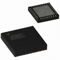
ATTINY261-20MU Atmel, ATTINY261-20MU Datasheet - Page 105

ATTINY261-20MU
Manufacturer Part Number
ATTINY261-20MU
Description
IC MCU AVR 2K FLASH 20MHZ 32-QFN
Manufacturer
Atmel
Series
AVR® ATtinyr
Specifications of ATTINY261-20MU
Core Processor
AVR
Core Size
8-Bit
Speed
20MHz
Connectivity
USI
Peripherals
Brown-out Detect/Reset, POR, PWM, WDT
Number Of I /o
16
Program Memory Size
2KB (1K x 16)
Program Memory Type
FLASH
Eeprom Size
128 x 8
Ram Size
128 x 8
Voltage - Supply (vcc/vdd)
2.7 V ~ 5.5 V
Data Converters
A/D 11x10b
Oscillator Type
Internal
Operating Temperature
-40°C ~ 85°C
Package / Case
32-VQFN Exposed Pad, 32-HVQFN, 32-SQFN, 32-DHVQFN
Processor Series
ATTINY2x
Core
AVR8
Data Bus Width
8 bit
Data Ram Size
128 B
Interface Type
2-Wire, SPI, USI
Maximum Clock Frequency
20 MHz
Number Of Programmable I/os
16
Number Of Timers
2
Maximum Operating Temperature
+ 85 C
Mounting Style
SMD/SMT
3rd Party Development Tools
EWAVR, EWAVR-BL
Development Tools By Supplier
ATAVRDRAGON, ATSTK500, ATSTK600, ATAVRISP2, ATAVRONEKIT
Minimum Operating Temperature
- 40 C
On-chip Adc
10 bit, 11 Channel
Package
32MLF EP
Device Core
AVR
Family Name
ATtiny
Maximum Speed
20 MHz
Operating Supply Voltage
3.3|5 V
For Use With
ATSTK600 - DEV KIT FOR AVR/AVR32ATAVRBC100 - REF DESIGN KIT BATTERY CHARGER770-1007 - ISP 4PORT ATMEL AVR MCU SPI/JTAGATSTK505 - ADAPTER KIT FOR 14PIN AVR MCU
Lead Free Status / RoHS Status
Lead free / RoHS Compliant
Available stocks
Company
Part Number
Manufacturer
Quantity
Price
Part Number:
ATTINY261-20MU
Manufacturer:
AVNET
Quantity:
20 000
- Current page: 105 of 242
- Download datasheet (5Mb)
2588E–AVR–08/10
Figure 12-14. PWM6 Mode, Single-slope Operation, Timing Diagram
The general I/O port function is overridden by the Output Compare value (OC1x / OC1x) from
the Dead Time Generator if either of the COM1x1:0 bits are set. The Output Compare pins can
also be overriden by the Output Compare Override Enable bits OC1OE5:OC1OE0. If an Over-
ride Enable bit is cleared, the actual value from the port register will be visible on the port pin
and, if the Override Enable bit is set, the Output Compare pin is allowed to be connected on the
port pin. The Output Compare Pin configurations are described in
Table
Table 12-5.
Table 12-6.
TCNT1
OCW1A
OC1A Pin
OC1OE1
OC1A Pin
OC1B Pin
OC1B Pin
OC1D Pin
OC1OE0
OC1OE2
OC1OE3
OC1OE4
OC1D Pin
OC1OE5
COM1A1
0
0
1
1
COM1B1
0
0
1
1
12-7.
Configuration of Output Compare Pins OC1A and OC1A in PWM6 Mode
Configuration of Output Compare Pins OC1B and OC1B in PWM6 Mode
COM1A0
0
1
0
1
COM1B0
0
1
0
1
OC1A Pin (PB0)
Disconnected
OC1A •
OC1A •
OC1A •
OC1B Pin (PB2)
Disconnected
OC1A •
OC1A •
OC1A •
OC1OE0
OC1OE0
OC1OE0
OC1OE2
OC1OE2
OC1OE2
OC1A Pin (PB1)
Disconnected
OC1A •
OC1A •
OC1A •
OC1B Pin (PB3)
Disconnected
OC1A •
OC1A •
OC1A •
Table
12-5,
OC1OE1
OC1OE1
OC1OE1
OC1OE3
OC1OE3
OC1OE3
Table 12-6
and
105
Related parts for ATTINY261-20MU
Image
Part Number
Description
Manufacturer
Datasheet
Request
R

Part Number:
Description:
Manufacturer:
Atmel Corporation
Datasheet:

Part Number:
Description:
Manufacturer:
Atmel Corporation
Datasheet:

Part Number:
Description:
IC MCU AVR 2K FLASH 20MHZ 20-DIP
Manufacturer:
Atmel
Datasheet:

Part Number:
Description:
MCU AVR 2K FLASH 15MHZ 32-QFN
Manufacturer:
Atmel
Datasheet:

Part Number:
Description:
MCU AVR 2KB FLASH 15MHZ 32-VQFN
Manufacturer:
Atmel
Datasheet:

Part Number:
Description:
IC MCU AVR 2K FLASH 20MHZ 20SOIC
Manufacturer:
Atmel
Datasheet:

Part Number:
Description:
Attiny261 8-bit Microcontroller With 2/4/8k Bytes In-system Programmable Flash
Manufacturer:
ATMEL Corporation
Datasheet:

Part Number:
Description:
IC MCU AVR 2K FLASH 20MHZ 20SOIC
Manufacturer:
Atmel
Datasheet:

Part Number:
Description:
IC MCU AVR 2K FLASH 20MHZ 32QFN
Manufacturer:
Atmel
Datasheet:

Part Number:
Description:
Manufacturer:
Atmel Corporation
Datasheet:


