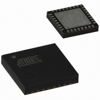
ATTINY261-20MU Atmel, ATTINY261-20MU Datasheet - Page 175

ATTINY261-20MU
Manufacturer Part Number
ATTINY261-20MU
Description
IC MCU AVR 2K FLASH 20MHZ 32-QFN
Manufacturer
Atmel
Series
AVR® ATtinyr
Specifications of ATTINY261-20MU
Core Processor
AVR
Core Size
8-Bit
Speed
20MHz
Connectivity
USI
Peripherals
Brown-out Detect/Reset, POR, PWM, WDT
Number Of I /o
16
Program Memory Size
2KB (1K x 16)
Program Memory Type
FLASH
Eeprom Size
128 x 8
Ram Size
128 x 8
Voltage - Supply (vcc/vdd)
2.7 V ~ 5.5 V
Data Converters
A/D 11x10b
Oscillator Type
Internal
Operating Temperature
-40°C ~ 85°C
Package / Case
32-VQFN Exposed Pad, 32-HVQFN, 32-SQFN, 32-DHVQFN
Processor Series
ATTINY2x
Core
AVR8
Data Bus Width
8 bit
Data Ram Size
128 B
Interface Type
2-Wire, SPI, USI
Maximum Clock Frequency
20 MHz
Number Of Programmable I/os
16
Number Of Timers
2
Maximum Operating Temperature
+ 85 C
Mounting Style
SMD/SMT
3rd Party Development Tools
EWAVR, EWAVR-BL
Development Tools By Supplier
ATAVRDRAGON, ATSTK500, ATSTK600, ATAVRISP2, ATAVRONEKIT
Minimum Operating Temperature
- 40 C
On-chip Adc
10 bit, 11 Channel
Package
32MLF EP
Device Core
AVR
Family Name
ATtiny
Maximum Speed
20 MHz
Operating Supply Voltage
3.3|5 V
For Use With
ATSTK600 - DEV KIT FOR AVR/AVR32ATAVRBC100 - REF DESIGN KIT BATTERY CHARGER770-1007 - ISP 4PORT ATMEL AVR MCU SPI/JTAGATSTK505 - ADAPTER KIT FOR 14PIN AVR MCU
Lead Free Status / RoHS Status
Lead free / RoHS Compliant
Available stocks
Company
Part Number
Manufacturer
Quantity
Price
Part Number:
ATTINY261-20MU
Manufacturer:
AVNET
Quantity:
20 000
- Current page: 175 of 242
- Download datasheet (5Mb)
18.6.2
2588E–AVR–08/10
Serial Programming Instruction set
Table 18-10. Minimum Wait Delay Before Writing the Next Flash or EEPROM Location
The instruction set is described in
Symbol
t
t
t
t
5. A: The EEPROM array is programmed one byte at a time by supplying the address and
6. Any memory location can be verified by using the Read instruction which returns the
7. At the end of the programming session, RESET can be set high to commence normal
8. Power-off sequence (if needed):
WD_FLASH
WD_EEPROM
WD_ERASE
WD_FUSE
interface before the Flash write operation completes can result in incorrect
programming.
data together with the appropriate Write instruction. An EEPROM memory location is
first automatically erased before new data is written. If polling (RDY/BSY) is not used,
the user must wait at least t
In a chip erased device, no 0xFFs in the data file(s) need to be programmed.
B: The EEPROM array is programmed one page at a time. The Memory page is loaded
one byte at a time by supplying the 2 LSB of the address and data together with the
Load EEPROM Memory Page instruction. The EEPROM Memory Page is stored by
loading the Write EEPROM Memory Page Instruction with the 6 MSB of the address.
When using EEPROM page access only byte locations loaded with the Load EEPROM
Memory Page instruction is altered. The remaining locations remain unchanged. If poll-
ing (RDY/BSY) is not used, the used must wait at least t
next page (See
be programmed.
content at the selected address at serial output MISO.
operation.
Set RESET to “1”.
Turn V
CC
power off.
Table
18-8). In a chip erased device, no 0xFF in the data file(s) need to
WD_EEPROM
Table 18-11 on page 176
before issuing the next byte. (See
Minimum Wait Delay
and
WD_EEPROM
4.5 ms
4.0 ms
9.0 ms
4.5 ms
Figure 18-2 on page
before issuing the
Table
18-10.)
177.
175
Related parts for ATTINY261-20MU
Image
Part Number
Description
Manufacturer
Datasheet
Request
R

Part Number:
Description:
Manufacturer:
Atmel Corporation
Datasheet:

Part Number:
Description:
Manufacturer:
Atmel Corporation
Datasheet:

Part Number:
Description:
IC MCU AVR 2K FLASH 20MHZ 20-DIP
Manufacturer:
Atmel
Datasheet:

Part Number:
Description:
MCU AVR 2K FLASH 15MHZ 32-QFN
Manufacturer:
Atmel
Datasheet:

Part Number:
Description:
MCU AVR 2KB FLASH 15MHZ 32-VQFN
Manufacturer:
Atmel
Datasheet:

Part Number:
Description:
IC MCU AVR 2K FLASH 20MHZ 20SOIC
Manufacturer:
Atmel
Datasheet:

Part Number:
Description:
Attiny261 8-bit Microcontroller With 2/4/8k Bytes In-system Programmable Flash
Manufacturer:
ATMEL Corporation
Datasheet:

Part Number:
Description:
IC MCU AVR 2K FLASH 20MHZ 20SOIC
Manufacturer:
Atmel
Datasheet:

Part Number:
Description:
IC MCU AVR 2K FLASH 20MHZ 32QFN
Manufacturer:
Atmel
Datasheet:

Part Number:
Description:
Manufacturer:
Atmel Corporation
Datasheet:


