PIC24F16KA101-I/MQ Microchip Technology, PIC24F16KA101-I/MQ Datasheet - Page 18
PIC24F16KA101-I/MQ
Manufacturer Part Number
PIC24F16KA101-I/MQ
Description
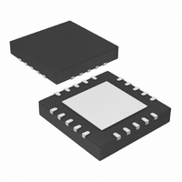
IC PIC MCU FLASH 2KX16 20-QFN
Manufacturer
Microchip Technology
Series
PIC® XLP™ 24Fr
Datasheets
1.MA240017.pdf
(254 pages)
2.PIC24F04KA201-ISS.pdf
(48 pages)
3.PIC24F16KA101-ISS.pdf
(18 pages)
Specifications of PIC24F16KA101-I/MQ
Program Memory Type
FLASH
Program Memory Size
16KB (5.5K x 24)
Package / Case
20-VQFN
Core Processor
PIC
Core Size
16-Bit
Speed
32MHz
Connectivity
I²C, IrDA, SPI, UART/USART
Peripherals
Brown-out Detect/Reset, POR, PWM, WDT
Number Of I /o
18
Eeprom Size
512 x 8
Ram Size
1.5K x 8
Voltage - Supply (vcc/vdd)
1.8 V ~ 3.6 V
Data Converters
A/D 9x10b
Oscillator Type
Internal
Operating Temperature
-40°C ~ 85°C
Processor Series
PIC24F
Core
PIC
Data Bus Width
16 bit
Data Ram Size
1.5 KB
Interface Type
I2C/IrDA/SPI/UART
Maximum Clock Frequency
32 MHz
Number Of Programmable I/os
18
Number Of Timers
3
Operating Supply Voltage
1.8 V to 3.6 V
Maximum Operating Temperature
+ 85 C
Mounting Style
SMD/SMT
3rd Party Development Tools
52713-733, 52714-737, 53276-922, EWDSPIC
Development Tools By Supplier
PG164130, DV164035, DV244005, DV164005, DM240001
Minimum Operating Temperature
- 40 C
On-chip Adc
9-ch x 10-bit
Lead Free Status / RoHS Status
Lead free / RoHS Compliant
Lead Free Status / RoHS Status
Lead free / RoHS Compliant, Lead free / RoHS Compliant
Available stocks
Company
Part Number
Manufacturer
Quantity
Price
Company:

Part Number:
PIC24F16KA101-I/MQ
Manufacturer:
SIEMENS
Quantity:
43


PIC24F16KA102 FAMILY
2.2
2.2.1
The use of decoupling capacitors on every pair of
power supply pins, such as V
AV
Consider the following criteria when using decoupling
capacitors:
• Value and type of capacitor: A 0.1 μF (100 nF),
• Placement on the printed circuit board: The
• Handling high-frequency noise: If the board is
• Maximizing performance: On the board layout
2.2.2
On boards with power traces running longer than six
inches in length, it is suggested to use a tank capacitor
for integrated circuits including microcontrollers to
supply a local power source. The value of the tank
capacitor should be determined based on the trace
resistance that connects the power supply source to
the device, and the maximum current drawn by the
device in the application. In other words, select the tank
capacitor so that it meets the acceptable voltage sag at
the device. Typical values range from 4.7 µF to 47 µF.
DS39927B-page 16
10-20V capacitor is recommended. The capacitor
should be a low-ESR device with a resonance
frequency in the range of 200 MHz and higher.
Ceramic capacitors are recommended.
decoupling capacitors should be placed as close
to the pins as possible. It is recommended to
place the capacitors on the same side of the
board as the device. If space is constricted, the
capacitor can be placed on another layer on the
PCB using a via; however, ensure that the trace
length from the pin to the capacitor is no greater
than 0.25 inch (6 mm).
experiencing high-frequency noise (upward of
tens of MHz), add a second ceramic type capaci-
tor in parallel to the above described decoupling
capacitor. The value of the second capacitor can
be in the range of 0.01 μF to 0.001 μF. Place this
second capacitor next to each primary decoupling
capacitor. In high-speed circuit designs, consider
implementing a decade pair of capacitances as
close to the power and ground pins as possible
(e.g., 0.1 μF in parallel with 0.001 μF).
from the power supply circuit, run the power and
return traces to the decoupling capacitors first, and
then to the device pins. This ensures that the
decoupling capacitors are first in the power chain.
Equally important is to keep the trace length
between the capacitor and the power pins to a
minimum, thereby reducing PCB trace inductance.
SS
is required.
Power Supply Pins
DECOUPLING CAPACITORS
TANK CAPACITORS
DD
, V
SS
, AV
DD
and
Preliminary
2.3
The
functions: device Reset, and device programming
and debugging. If programming and debugging are
not required in the end application, a direct
connection to V
addition of other components, to help increase the
application’s resistance to spurious Resets from
voltage
configuration is shown in Figure 2-1. Other circuit
designs may be implemented, depending on the
application’s requirements.
During programming and debugging, the resistance
and capacitance that can be added to the pin must
be considered. Device programmers and debuggers
drive the MCLR pin. Consequently, specific voltage
levels (V
not be adversely affected. Therefore, specific values
of R1 and C1 will need to be adjusted based on the
application and PCB requirements. For example, it is
recommended that the capacitor C1 be isolated from
the MCLR pin during programming and debugging
operations by using a jumper (Figure 2-2). The
jumper is replaced for normal run-time operations.
Any components associated with the MCLR pin
should be placed within 0.25 inch (6 mm) of the pin.
FIGURE 2-2:
Note 1: R1 ≤ 10 kΩ is recommended. A suggested
MCLR
2: R2 ≤ 470Ω will limit any current flowing into
Master Clear (MCLR) Pin
IH
sags,
and V
V
starting value is 10 kΩ. Ensure that the
MCLR pin V
MCLR from the external capacitor C, in the
event of MCLR pin breakdown, due to
Electrostatic Discharge (ESD) or Electrical
Overstress (EOS). Ensure that the MCLR pin
V
IH
DD
R1
pin
JP
and V
C1
DD
IL
may
) and fast signal transitions must
may be all that is required. The
provides
IL
EXAMPLE OF MCLR PIN
CONNECTIONS
specifications are met.
IH
R2
© 2009 Microchip Technology Inc.
and V
be
MCLR
IL
beneficial.
PIC24FXXXX
two
specifications are met.
specific
A
device
typical
Related parts for PIC24F16KA101-I/MQ
Image
Part Number
Description
Manufacturer
Datasheet
Request
R

Part Number:
Description:
Manufacturer:
Microchip Technology Inc.
Datasheet:
Part Number:
Description:
Manufacturer:
Microchip Technology Inc.
Datasheet:
Part Number:
Description:
Manufacturer:
Microchip Technology Inc.
Datasheet:
Part Number:
Description:
Manufacturer:
Microchip Technology Inc.
Datasheet:
Part Number:
Description:
Manufacturer:
Microchip Technology Inc.
Datasheet:
Part Number:
Description:
Manufacturer:
Microchip Technology Inc.
Datasheet:
Part Number:
Description:
Manufacturer:
Microchip Technology Inc.
Datasheet:
Part Number:
Description:
Manufacturer:
Microchip Technology Inc.
Datasheet: