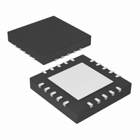
PIC24F16KA101-I/MQ Microchip Technology, PIC24F16KA101-I/MQ Datasheet - Page 63

PIC24F16KA101-I/MQ
Manufacturer Part Number
PIC24F16KA101-I/MQ
Description
IC PIC MCU FLASH 2KX16 20-QFN
Manufacturer
Microchip Technology
Series
PIC® XLP™ 24Fr
Datasheets
1.MA240017.pdf
(254 pages)
2.PIC24F04KA201-ISS.pdf
(48 pages)
3.PIC24F16KA101-ISS.pdf
(18 pages)
Specifications of PIC24F16KA101-I/MQ
Program Memory Type
FLASH
Program Memory Size
16KB (5.5K x 24)
Package / Case
20-VQFN
Core Processor
PIC
Core Size
16-Bit
Speed
32MHz
Connectivity
I²C, IrDA, SPI, UART/USART
Peripherals
Brown-out Detect/Reset, POR, PWM, WDT
Number Of I /o
18
Eeprom Size
512 x 8
Ram Size
1.5K x 8
Voltage - Supply (vcc/vdd)
1.8 V ~ 3.6 V
Data Converters
A/D 9x10b
Oscillator Type
Internal
Operating Temperature
-40°C ~ 85°C
Processor Series
PIC24F
Core
PIC
Data Bus Width
16 bit
Data Ram Size
1.5 KB
Interface Type
I2C/IrDA/SPI/UART
Maximum Clock Frequency
32 MHz
Number Of Programmable I/os
18
Number Of Timers
3
Operating Supply Voltage
1.8 V to 3.6 V
Maximum Operating Temperature
+ 85 C
Mounting Style
SMD/SMT
3rd Party Development Tools
52713-733, 52714-737, 53276-922, EWDSPIC
Development Tools By Supplier
PG164130, DV164035, DV244005, DV164005, DM240001
Minimum Operating Temperature
- 40 C
On-chip Adc
9-ch x 10-bit
Lead Free Status / RoHS Status
Lead free / RoHS Compliant
Lead Free Status / RoHS Status
Lead free / RoHS Compliant, Lead free / RoHS Compliant
Available stocks
Company
Part Number
Manufacturer
Quantity
Price
Company:
Part Number:
PIC24F16KA101-I/MQ
Manufacturer:
SIEMENS
Quantity:
43
7.2.1
The oscillator start-up circuitry and its associated delay
timers are not linked to the device Reset delays that
occur at power-up. Some crystal circuits (especially
low-frequency crystals) will have a relatively long
start-up time. Therefore, one or more of the following
conditions is possible after SYSRST is released:
• The oscillator circuit has not begun to oscillate.
• The Oscillator Start-up Timer has not expired (if a
• The PLL has not achieved a lock (if PLL is used).
The device will not begin to execute code until a valid
clock source has been released to the system. There-
fore, the oscillator and PLL start-up delays must be
considered when the Reset delay time must be known.
7.2.2
If the FSCM is enabled, it will begin to monitor the
system clock source when SYSRST is released. If a
valid clock source is not available at this time, the
device will automatically switch to the FRC Oscillator
and the user can switch to the desired crystal oscillator
in the Trap Service Routine (TSR).
7.3
Most of the Special Function Registers (SFRs) associ-
ated with the PIC24F CPU and peripherals are reset to a
particular value at a device Reset. The SFRs are
grouped by their peripheral or CPU function and their
Reset values are specified in each section of this manual.
The Reset value for each SFR does not depend on the
type of Reset with the exception of four registers. The
Reset value for the Reset Control register, RCON, will
depend on the type of device Reset. The Reset value
for the Oscillator Control register, OSCCON, will
depend on the type of Reset and the programmed
values of the FNOSC bits in the Flash Configuration
Word (FOSCSEL); see Table 7-2. The RCFGCAL and
NVMCON registers are only affected by a POR.
7.4
Deep Sleep BOR is a very low-power BOR circuitry,
used when the device is in Deep Sleep mode. Due to
low-current consumption, accuracy may vary.
The DSBOR trip point is around 2.0V. DSBOR is
enabled
DSLPBOR will re-arm the POR to ensure the device will
reset if V
© 2009 Microchip Technology Inc.
crystal oscillator is used).
DD
Special Function Register Reset
States
Deep Sleep BOR (DSBOR)
by
POR AND LONG OSCILLATOR
START-UP TIMES
FAIL-SAFE CLOCK MONITOR
(FSCM) AND DEVICE RESETS
drops below the POR threshold.
configuring
FDS<DSLPBOR>
=
Preliminary
1.
PIC24F16KA102 FAMILY
7.5
The PIC24F16KA102 family devices implement a BOR
circuit, which provides the user several configuration
and power-saving options. The BOR is controlled by
the <BORV1:BORV0> and (BOREN<1:0>) Configura-
tion bits (FPOR<6:5,1:0>). There are a total of four
BOR configurations, which are provided in Table 7-3.
The BOR threshold is set by the BORV<1:0> bits. If
BOR is enabled (any values of BOREN<1:0>, except
‘00’), any drop of V
reset the device. The chip will remain in BOR until V
rises above threshold.
If the Power-up Timer is enabled, it will be invoked after
V
in Reset for an additional time delay, T
below the threshold while the power-up timer is running.
The chip goes back into a BOR and the Power-up Timer
will be initialized. Once V
the Power-up Timer will execute the additional time
delay.
BOR and the Power-up Timer are independently
configured. Enabling the BOR Reset does not
automatically enable the PWRT.
7.5.1
When BOREN<1:0> = 01, the BOR can be enabled or
disabled by the user in software. This is done with the
control bit, SBOREN (RCON<13>). Setting SBOREN
enables the BOR to function as previously described.
Clearing the SBOREN disables the BOR entirely. The
SBOREN bit operates only in this mode; otherwise, it is
read as ‘0’.
Placing BOR under software control gives the user the
additional flexibility of tailoring the application to its
environment without having to reprogram the device to
change the BOR configuration. It also allows the user
to tailor the incremental current that the BOR con-
sumes. While the BOR current is typically very small, it
may have some impact in low-power applications.
DD
Note:
rises above the threshold; it, then, will keep the chip
Brown-out Reset (BOR)
SOFTWARE ENABLED BOR
Even when the BOR is under software
control, the BOR Reset voltage level is still
set by the BORV<1:0> Configuration bits.
It can not be changed in software.
DD
below the set threshold point will
DD
rises above the threshold,
PWRT
DS39927B-page 61
, if V
DD
drops
DD


