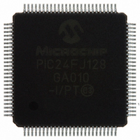
PIC24FJ128GA010-I/PT Microchip Technology, PIC24FJ128GA010-I/PT Datasheet - Page 181

PIC24FJ128GA010-I/PT
Manufacturer Part Number
PIC24FJ128GA010-I/PT
Description
IC PIC MCU FLASH 128K 100TQFP
Manufacturer
Microchip Technology
Series
PIC® 24Fr
Datasheets
1.PIC24FJ16GA002-ISS.pdf
(52 pages)
2.PIC24FJ64GA006-IPT.pdf
(240 pages)
3.PIC24FJ64GA006-IPT.pdf
(22 pages)
4.PIC24FJ128GA008-IPT.pdf
(12 pages)
5.PIC24FJ128GA006-IPT.pdf
(231 pages)
6.PIC24FJ128GA010-IPT.pdf
(230 pages)
Specifications of PIC24FJ128GA010-I/PT
Core Size
16-Bit
Program Memory Size
128KB (43K x 24)
Core Processor
PIC
Speed
16MHz
Connectivity
I²C, PMP, SPI, UART/USART
Peripherals
Brown-out Detect/Reset, POR, PWM, WDT
Number Of I /o
84
Program Memory Type
FLASH
Ram Size
8K x 8
Voltage - Supply (vcc/vdd)
2 V ~ 3.6 V
Data Converters
A/D 16x10b
Oscillator Type
Internal
Operating Temperature
-40°C ~ 85°C
Package / Case
100-TFQFP
Controller Family/series
PIC24
No. Of I/o's
84
Ram Memory Size
8KB
Cpu Speed
32MHz
No. Of Timers
5
No. Of Pwm Channels
5
Embedded Interface Type
EUART, I2C, PSP, SPI
Rohs Compliant
Yes
Processor Series
PIC24FJ
Core
PIC
Data Bus Width
16 bit
Data Ram Size
8 KB
Interface Type
SPI, I2C, USART
Maximum Clock Frequency
16 MHz
Number Of Programmable I/os
54
Number Of Timers
5
Maximum Operating Temperature
+ 85 C
Mounting Style
SMD/SMT
3rd Party Development Tools
52713-733, 52714-737, 53276-922, EWDSPIC
Development Tools By Supplier
PG164130, DV164035, DV244005, DV164005, PG164120, DM240001, DM240011
Minimum Operating Temperature
- 40 C
On-chip Adc
10 bit, 16 Channel
Package
100TQFP
Device Core
PIC
Family Name
PIC24
Maximum Speed
16 MHz
Operating Supply Voltage
2.5|3.3 V
Lead Free Status / RoHS Status
Lead free / RoHS Compliant
For Use With
DM240011 - KIT STARTER MPLAB FOR PIC24F MCUAC164333 - MODULE SKT FOR PM3 100QFPDV164033 - KIT START EXPLORER 16 MPLAB ICD2MA160011 - DAUGHTER BOARD PICDEM LCD 16F91XDM240001 - BOARD DEMO PIC24/DSPIC33/PIC32
Eeprom Size
-
Lead Free Status / Rohs Status
Details
Available stocks
Company
Part Number
Manufacturer
Quantity
Price
Company:
Part Number:
PIC24FJ128GA010-I/PT
Manufacturer:
Microchi
Quantity:
627
Company:
Part Number:
PIC24FJ128GA010-I/PT
Manufacturer:
MICROCHIP
Quantity:
212
Company:
Part Number:
PIC24FJ128GA010-I/PT
Manufacturer:
Microchip Technology
Quantity:
10 000
23.0
PIC24FJ128GA
features intended to maximize application flexibility and
reliability, and minimize cost through elimination of
external components. These are:
• Flexible Configuration
• Watchdog Timer (WDT)
• Code Protection
• JTAG Boundary Scan Interface
• In-Circuit Serial Programming
• In-Circuit Emulation
23.1
The Configuration bits can be programmed (read as
‘0’), or left unprogrammed (read as ‘1’), to select vari-
ous device configurations. These bits are mapped
starting at program memory location F80000h. A com-
plete list is shown in Table 23-1. A detailed explanation
of the various bit functions is provided in Register 23-1
through Register 23-4.
Note that address F80000h is beyond the user program
memory space. In fact, it belongs to the configuration
memory space (800000h-FFFFFFh) which can only be
accessed using table reads and table writes.
23.1.1
In PIC24FJ128GA family devices, the configuration
bytes are implemented as volatile memory. This means
that configuration data must be programmed each time
the device is powered up. Configuration data is stored
in the two words at the top of the on-chip program
memory space, known as the Flash Configuration
Words. Their specific locations are shown in
Table 23-1. These are packed representations of the
actual device Configuration bits, whose actual
locations are distributed among five locations in config-
uration space. The configuration data is automatically
loaded from the Flash Configuration Words to the
proper Configuration registers during device Resets.
© 2006 Microchip Technology Inc.
Note:
SPECIAL FEATURES
Configuration Bits
This data sheet summarizes the features
of this group of PIC24FJ devices. It is not
intended to be a comprehensive reference
source.
CONSIDERATIONS FOR
CONFIGURING PIC24FJ128GA
FAMILY DEVICES
family
devices
include
several
Preliminary
PIC24FJ128GA FAMILY
TABLE 23-1:
When creating applications for these devices, users
should always specifically allocate the location of the
Flash Configuration Word for configuration data. This is
to make certain that program code is not stored in this
address when the code is compiled.
The volatile memory cells used for the Configuration
bits always reset to ‘1’ on Power-on Resets. For all
other type of Reset events, the previously programmed
values are maintained and used without reloading from
program memory.
The upper byte of both Flash Configuration Words in
program memory should always be ‘1111 1111’. This
makes them appear to be NOP instructions in the
remote event that their locations are ever executed by
accident. Since Configuration bits are not implemented
in the corresponding locations, writing ‘1’s to these
locations has no effect on device operation.
To prevent inadvertent configuration changes during
code execution, all programmable Configuration bits
are write-once. After a bit is initially programmed during
a power cycle, it cannot be written to again. Changing
a device configuration requires that power to the device
be cycled.
PIC24FJ64GA
PIC24FJ96GA
PIC24FJ128GA
Device
FLASH CONFIGURATION
WORDS LOCATIONS FOR
PIC24FJ128GA FAMILY
DEVICES
00ABFEh
00FFFEh
0157FEh
Configuration Word
1
Addresses
DS39747C-page 179
00ABFCh
00FFFCh
0157FCh
2


