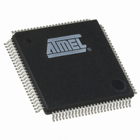
AT91M40800-33AU Atmel, AT91M40800-33AU Datasheet - Page 27

AT91M40800-33AU
Manufacturer Part Number
AT91M40800-33AU
Description
IC ARM7 MCU 100 LQFP
Manufacturer
Atmel
Series
AT91SAMr
Specifications of AT91M40800-33AU
Core Processor
ARM7
Core Size
16/32-Bit
Speed
33MHz
Connectivity
EBI/EMI, UART/USART
Peripherals
POR, WDT
Number Of I /o
32
Program Memory Type
ROMless
Ram Size
8K x 8
Voltage - Supply (vcc/vdd)
1.8 V ~ 3.6 V
Oscillator Type
External
Operating Temperature
-40°C ~ 85°C
Package / Case
100-LQFP
Package
100TQFP
Device Core
ARM7TDMI
Family Name
91M
Maximum Speed
33 MHz
Operating Supply Voltage
2.5|3.3 V
Data Bus Width
32 Bit
Number Of Programmable I/os
32
Interface Type
EBI/USART
Number Of Timers
3
Processor Series
AT91Mx
Core
ARM7TDMI
Data Ram Size
8 KB
Maximum Clock Frequency
33 MHz
Maximum Operating Temperature
+ 85 C
Mounting Style
SMD/SMT
3rd Party Development Tools
JTRACE-ARM-2M, MDK-ARM, RL-ARM, ULINK2
Minimum Operating Temperature
- 40 C
Eeprom Memory
0 Bytes
Input Output
32
Interface
EBI/EMI, UART/USART
Ios
32
Memory Type
ROMless
Number Of Bits
32
Package Type
100-pin LQFP
Programmable Memory
0 Bytes
Timers
3-16-bit
Voltage, Range
1.8-3.6 V
Cpu Family
91M
Device Core Size
32b
Frequency (max)
33MHz
Program Memory Size
Not Required
Total Internal Ram Size
8KB
# I/os (max)
32
Number Of Timers - General Purpose
3
Operating Supply Voltage (typ)
2.5/3.3V
Operating Supply Voltage (max)
3.6V
Operating Supply Voltage (min)
1.8V
Instruction Set Architecture
RISC
Operating Temp Range
-40C to 85C
Operating Temperature Classification
Industrial
Mounting
Surface Mount
Pin Count
100
Lead Free Status / RoHS Status
Lead free / RoHS Compliant
Eeprom Size
-
Program Memory Size
-
Data Converters
-
Lead Free Status / Rohs Status
Lead free / RoHS Compliant
Available stocks
Company
Part Number
Manufacturer
Quantity
Price
Company:
Part Number:
AT91M40800-33AU
Manufacturer:
ATMEL
Quantity:
1 000
Company:
Part Number:
AT91M40800-33AU
Manufacturer:
ATMEL
Quantity:
346
Part Number:
AT91M40800-33AU
Manufacturer:
ATMEL/爱特梅尔
Quantity:
20 000
Read Protocols
Standard Read Protocol
Early Read Protocol
Early Read Wait State
1354D–ATARM–08/02
The EBI provides two alternative protocols for external memory read access: standard
and early read. The difference between the two protocols lies in the timing of the NRD
(read cycle) waveform.
The protocol is selected by the DRP field in EBI_MCR (Memory Control Register) and is
valid for all memory devices. Standard read protocol is the default protocol after reset.
Note:
Standard read protocol implements a read cycle in which NRD and NWE are similar.
Both are active during the second half of the clock cycle. The first half of the clock cycle
allows time to ensure completion of the previous access as well as the output of address
and NCS before the read cycle begins.
During a standard read protocol, external memory access, NCS is set low and ADDR is
valid at the beginning of the access while NRD goes low only in the second half of the
master clock cycle to avoid bus conflict (see Figure 14). NWE is the same in both proto-
cols. NWE always goes low in the second half of the master clock cycle (see Figure 15).
Early read protocol provides more time for a read access from the memory by asserting
NRD at the beginning of the clock cycle. In the case of successive read cycles in the
same memory, NRD remains active continuously. Since a read cycle normally limits the
speed of operation of the external memory system, early read protocol can allow a
faster clock frequency to be used. However, an extra wait state is required in some
cases to avoid contentions on the external bus.
In early read protocol, an early read wait state is automatically inserted when an exter-
nal write cycle is followed by a read cycle to allow time for the write cycle to end before
the subsequent read cycle begins (see Figure 16). This wait state is generated in addi-
tion to any other programmed wait states (i.e. data float wait).
No wait state is added when a read cycle is followed by a write cycle, between consecu-
tive accesses of the same type or between external and internal memory accesses.
Early read wait states affect the external bus only. They do not affect internal bus timing.
Figure 14. Standard Read Protocol
In the following waveforms and descriptions, NRD represents NRD and NOE since the
two signals have the same waveform. Likewise, NWE represents NWE, NWR0 and
NWR1 unless NWR0 and NWR1 are otherwise represented. ADDR represents A0 - A23
and/or A1 - A23.
or
ADDR
MCKI
NWE
NCS
NRD
AT91X40 Series
27


